Graphene
From Wikipedia, the free encyclopedia
Not to be confused with Grapheme.
| This article may be too technical for most readers to understand. (December 2012) |

Graphene is a substance composed of pure carbon, with atoms arranged in a regular hexagonal pattern similar to graphite, but in a one-atom thick sheet. It is very light, with a 1-square-meter sheet weighing only 0.77 milligrams.
It is an allotrope of carbon whose structure is a single planar sheet of sp2-bonded carbon atoms, that are densely packed in a honeycomb crystal lattice.[1] The term graphene was coined as a combination of graphite and the suffix -ene by Hanns-Peter Boehm,[2] who described single-layer carbon foils in 1962.[3] Graphene is most easily visualized as an atomic-scale chicken wire made of carbon atoms and their bonds. The crystalline or "flake" form of graphite consists of many graphene sheets stacked together.
The carbon-carbon bond length in graphene is about 0.142 nanometers.[4] Graphene sheets stack to form graphite with an interplanar spacing of 0.335 nm. Graphene is the basic structural element of some carbon allotropes including graphite, charcoal, carbon nanotubes and fullerenes. It can also be considered as an indefinitely large aromatic molecule, the limiting case of the family of flat polycyclic aromatic hydrocarbons.
There is an analog of graphene composed of silicon called silicene.
The Nobel Prize in Physics for 2010 was awarded to Andre Geim and Konstantin Novoselov at the University of Manchester "for groundbreaking experiments regarding the two-dimensional material graphene".[5] In 2013, graphene researchers led by Prof. Jari Kinaret from Sweden's Chalmers University, secured a €1 billion grant from the European Union.[6]
[edit]Description
One definition given in a recent review on graphene is:
A previous definition is:
A single carbon layer of the graphitic structure can be considered as the final member of the series naphthalene, anthracene, coronene, etc. and the term graphene should therefore be used to designate the individual carbon layers in graphite intercalation compounds. Use of the term "graphene layer" is also considered for the general terminology of carbons.[2]
The IUPAC compendium of technology states: "previously, descriptions such as graphite layers, carbon layers, or carbon sheets have been used for the term graphene... it is incorrect to use for a single layer a term which includes the term graphite, which would imply a three-dimensional structure. The term graphene should be used only when the reactions, structural relations or other properties of individual layers are discussed."[7] In this regard, graphene has been referred to as an infinite alternant (only six-member carbon ring) polycyclic aromatic hydrocarbon (PAH). The largest known isolated molecule of this type consists of 222 atoms and is 10 benzene rings across.[8] It has proven difficult to synthesize even slightly bigger molecules, and they still remain "a dream of many organic and polymer chemists".[9]
Furthermore, ab initio calculations show that a graphene sheet is thermodynamically unstable with respect to other fullerene structures if its size is less than about 20 nm (“graphene is the least stable structure until about 6000 atoms”) and becomes the most stable one (as within graphite) only for sizes larger than 24,000 carbon atoms.[10] The flat graphene sheet is also known to be unstable with respect to scrolling i.e. curling up, which is its lower-energy state.[11]
A definition of "isolated or free-standing graphene" has also recently been proposed: "graphene is a single atomic plane of graphite, which – and this is essential – is sufficiently isolated from its environment to be considered free-standing."[12] This definition is narrower than the definitions given above and refers to cleaved, transferred and suspended graphene monolayers.[citation needed]
Other forms of graphene, such as graphene grown on various metals, can also become free-standing if, for example, suspended or transferred to silicon dioxide (SiO2). A new example of isolated graphene is graphene on silicon carbide (SiC) after its passivation with hydrogen.[13]
[edit]Occurrence and production

In essence, graphene is an isolated atomic plane of graphite. From this perspective, graphene has been known since the invention of X-ray crystallography. Graphene planes become even better separated in intercalated graphite compounds. In 2004, physicists at the University of Manchester and the Institute for Microelectronics Technology, Chernogolovka, Russia, first isolated individual graphene planes by using adhesive tape.[14] They also measured electronic properties of the obtained flakes and showed their unique properties.[15] In 2005 the same Manchester Geim group together with the Philip Kimgroup from Columbia University (see the History section) demonstrated that quasiparticles in graphene were massless Dirac fermions. These discoveries led to an explosion of interest in graphene.
Since then, hundreds of researchers have entered the area, resulting in an extensive search for relevant earlier papers. The Manchester researchers themselves published the first literature review.[1] They cite several papers in which graphene or ultra-thin graphitic layers were epitaxially grown on various substrates. Also, they note a number of pre-2004 reports in which intercalated graphite compounds were studied in a transmission electron microscope. In the latter case, researchers occasionally observed extremely thin graphitic flakes ("few-layer graphene" and possibly even individual layers). An early detailed study on few-layer graphene dates back to 1962.[16] The earliest TEM images of few-layer graphene were published by G. Ruess and F. Vogt in 1948.[17] In 1859 Benjamin Collins Brodie was aware of the highly lamellar structure of thermally reduced graphite oxide.[18] It was studied in detail by V. Kohlschütter and P. Haenni in 1918, who also described the properties of graphite oxide paper.[19]
It is now well known that tiny fragments of graphene sheets are produced (along with quantities of other debris) whenever graphite is abraded, such as when drawing a line with a pencil.[14] There was little interest in this graphitic residue before 2004/05 and, therefore, the discovery of graphene is often attributed to Andre Geim and colleagues[20] who introduced graphene in its modern incarnation.
In 2008, graphene produced by exfoliation was one of the most expensive materials on Earth, with a sample that can be placed at the cross section of a human hair costing more than $1,000 as of April 2008 (about $100,000,000/cm2).[14] Since then, exfoliation procedures have been scaled up, and now companies sell graphene in large quantities.[21][22] On the other hand, the price of epitaxial graphene on SiC is dominated by the substrate price, which is approximately $100/cm2 as of 2009. Byung Hee Hong and his team in South Korea pioneered the synthesis of large-scale graphene films using chemical vapour deposition (CVD) on thin nickel layers, which triggered chemical researches toward the practical applications of graphene,[23][24] with wafer sizes up to 30 inches (760 mm) reported.[25]
In 2011 the Institute of Electronic Materials Technology and Department of Physics, Warsaw University announced a joint development of acquisition technology of large pieces of graphene with the best quality so far.[26][27]
In the literature, specifically that of the surface science community, graphene has also been commonly referred to as monolayer graphite. This community has intensely studied epitaxial graphene on various surfaces (over 300 articles prior to 2004). In some cases, these graphene layers are coupled to the surfaces weakly enough (by Van der Waals forces) to retain the two dimensional electronic band structure of isolated graphene,[28][29] as also happens[15] with exfoliated graphene flakes with regard to SiO2. An example of weakly coupled epitaxial graphene is the one grown on SiC (see below).
[edit]Exfoliated graphene
In 2004, the Manchester group obtained graphene by micro-mechanical alleviation of graphite. They used adhesive tape to repeatedly split graphite crystals into increasingly thinner pieces (however, filed in 2002 US Patent 6,667,100 describes the process in detail to achieve a graphite thickness of 0.01 thousandth of an inch). The tape with attached optically transparent flakes was dissolved in acetone, and, after a few further steps, the flakes including monolayers were sedimented on a silicon wafer. Individual atomic planes were then hunted with an optical microscope. A year later, the researchers simplified the technique and started using dry deposition, avoiding the stage when graphene floated in a liquid. Relatively large crystallites (first, only a few micrometres in size but eventually larger than 1 mm and visible to the naked eye) were obtained with the technique. It is often referred to as a scotch tape or drawing method. The latter name appeared because the dry deposition resembles drawing with a piece of graphite.[30] The key for the success probably was the use of high-throughput visual recognition of graphene on a properly chosen substrate, which provides a small but noticeable optical contrast. The optical properties section below contains a photograph of what graphene looks like.
The isolation of graphene led to the current research boom. Previously, free-standing atomic planes were often "presumed not to exist"[15] because they are thermodynamically unstable on a nanometer scale[10] and, if unsupported, have a tendency to scroll and buckle.[9] It is currently believed that intrinsic microscopic roughening on the scale of 1 nm could be important for the stability of purely 2D crystals.[31]
There were a number of previous attempts to make atomically thin graphitic films by using exfoliation techniques similar to the drawing method. Multilayer samples down to 10 nm in thickness were obtained. These efforts were reviewed in 2007.[1] Furthermore, a couple of very old papers were recently unearthed[16] in which researchers tried to isolate graphene starting with intercalated compounds (see History and experimental discovery). These papers reported the observation of very thin graphitic fragments (possibly monolayers) by transmission electron microscopy. Neither of the earlier observations was sufficient to "spark the graphene gold rush", until the Science paper did so by reporting not only macroscopic samples of extracted atomic planes but, importantly, their unusual properties such as the bipolar transistor effect, ballistic transport of charges, large quantum oscillations, etc. The discovery of such interesting qualities intrinsic to graphene gave an immediate boost to further research and several groups quickly repeated the initial result and moved further. These breakthroughs also helped to attract attention to other production techniques, such as epitaxial growth of ultra-thin graphitic films. In particular, it has later been found that graphene monolayers grown on SiC and Ir are weakly coupled to these substrates (how weakly remains debated) and the graphene–substrate interaction can be passivated further.[13]
Not only graphene but also free-standing atomic planes of boron nitride, mica, dichalcogenides and complex oxides were obtained by using the drawing method.[32] Unlike graphene, the other 2D materials have so far attracted surprisingly little attention.
[edit]Epitaxial growth on silicon carbide
Main article: Carbide-derived Carbon
Another method of obtaining graphene is to heat silicon carbide (SiC) to high temperatures (>1,100 °C) under low pressures (~10−6 torr) to reduce it to graphene.[33] This process produces epitaxial graphene with dimensions dependent upon the size of the SiC substrate (wafer). The face of the SiC used for graphene formation, silicon- or carbon-terminated, highly influences the thickness, mobility and carrier density of the graphene.
Many important graphene properties have been identified in graphene produced by this method. For example, the electronic band-structure (so-called Dirac cone structure) has been first visualized in this material.[34][35][36] Weak anti-localization is observed in this material and not in exfoliated graphene produced by the pencil-trace method.[37]Extremely large, temperature-independent mobilities have been observed in SiC-epitaxial graphene. They approach those in exfoliated graphene placed on silicon oxide but still much lower than mobilities in suspended graphene produced by the drawing method. It was recently shown that even without being transferred, graphene on SiC exhibits the properties of massless Dirac fermions such as the anomalous quantum Hall effect.[38][39][40][41][42]
The weak van der Waals force that provides the cohesion of multilayer graphene stacks does not always affect the electronic properties of the individual graphene layers in the stack. That is, while the electronic properties of certain multilayered epitaxial graphenes are identical to that of a single graphene layer,[43] in other cases the properties are affected[34][35] as they are for graphene layers in bulk graphite. This effect is theoretically well understood and is related to the symmetry of the interlayer interactions.[43]
Epitaxial graphene on SiC can be patterned using standard microelectronics methods. The possibility of large integrated electronics on SiC-epitaxial graphene was first proposed in 2004,[44] and a patent for graphene-based electronics was filed provisionally in 2003 and issued in 2006.[45] Since then, important advances have been made. In 2008, researchers at MIT Lincoln Lab produced hundreds of transistors on a single chip[46] and in 2009, very high frequency transistors were produced at the Hughes Research Laboratories on monolayer graphene on SiC.[47] Band gap of the epitaxial graphene can be tuned by irradiating with laser beams; modified graphene has a lot of advantages in device application.[48]
[edit]Epitaxial growth on metal substrates
This method uses source and the atomic structure of a metal substrate to seed the growth of the graphene (epitaxial growth). Graphene grown on ruthenium doesn't typically yield a sample with a uniform thickness of graphene layers, and bonding between the bottom graphene layer and the substrate may affect the properties of the carbon layers.[49]On the other hand, graphene grown on iridium is very weakly bonded, uniform in thickness, and can be made highly ordered. Like on many other substrates, graphene on iridium is slightly rippled. Due to the long-range order of these ripples, generation of minigaps in the electronic band-structure (Dirac cone) becomes visible.[50] High-quality sheets of few-layer graphene exceeding 1 cm2 (0.2 sq in) in area have been synthesized via chemical vapor deposition on thin nickel films with methane as a carbon source. These sheets have been successfully transferred to various substrates, demonstrating viability for numerous electronic applications.[25][38]
An improvement of this technique has employed copper foil; at very low pressure, the growth of graphene automatically stops after a single graphene layer forms, and arbitrarily large graphene films can be created.[25][51] The aforementioned single layer growth is also due to the low concentration of carbon in methane. Larger hydrocarbon gasses, such as ethane and propane, will lead to the growth of bilayer graphene.[52] In this light, it is obvious that at atmospheric-pressure CVD growth, multilayer graphene will also form on copper (similar to that grown on nickel films).[53] Growth of graphene has been demonstrated at temperatures compatible with conventional CMOS processing, using a nickel-based alloy with gold as catalysts.[54]
[edit]Graphite oxide reduction
Graphite oxide reduction was probably historically the first method of graphene synthesis. P. Boehm reported monolayer flakes of reduced graphene oxide already in 1962.[55] In this early work existence of monolayer reduced graphene oxide flakes was demonstrated. The contribution of Boehm was recently acknowledged by Nobel prize winner for graphene research, Andre Geim: (Many Pioneers in Graphene Discovery). Graphite oxide exfoliation can be achieved by rapid heating and yields highly dispersed carbon powder with a few percent of graphene flakes. Reduction of graphite oxide monolayer films e.g. by hydrazine, annealing in argon/hydrogen was reported to yield graphene films. However, the quality of graphene produced by graphite oxide reduction is lower compared to e.g. scotch-tape graphene due to incomplete removal of various functional groups by existing reduction methods. Recently, reduction and exfoliation of graphite oxide by focused solar radiation was reported with less oxygen functionalities.[56] Some spectroscopic analysis of reduced graphene oxide can be found in the literature.[57] Applying a layer of graphite oxide film to a DVD disc and burning it in a DVD writer resulted in a thin graphene film with high electrical conductivity (1738 siemens per meter) and specific surface area (1520 square meters per gram), besides being highly resistant and malleable.[58][59] In February 2013 researchers from UCLA, led by professor Richard Kaner, announced a novel technique to produce graphene supercapacitors based on the DVD burner approach.[60]
[edit]Growth from metal-carbon melts
The general idea in this process is to dissolve carbon atoms inside a transition metal melt at a certain temperature, and then allow the dissolved carbon to precipitate out at lower temperatures as single layer graphene (SLG).[61] The metal is first melted in contact with a carbon source. This source could be the graphite crucible inside which the melting process is carried out or it could be the graphite powder or chunk sources, which are simply placed in contact with the melt. Keeping the melt in contact with carbon source at a given temperature will give rise to dissolution and saturation of carbon atoms in the melt based on the binary phase diagram of metal-carbon. Upon lowering the temperature, solubility of the carbon in the molten metal will decrease and the excess amount of carbon will precipitate on top of the melt. The floating layer can be either skimmed or allowed to freeze for removal afterwards. Different morphology including thick graphite, few layer graphene (FLG) and SLG were observed on metal substrate. The Raman spectroscopy proved that SLG has been successfully grown on nickel substrate. The SLG Raman spectrum featured no D and D′ band, indicating the pristine and high-quality nature of SLG. Among transition metals, nickel provides a better substrate for growing SLG. Since nickel is not Raman active, the direct Raman spectroscopy of graphene layers on top of the nickel is achievable. The graphene-metal composite could be utilized in thermal interface materials for thermal management applications.[61]
[edit]Pyrolysis of sodium ethoxide
A 2008 publication described a process for producing gram-quantities of graphene, by the reduction of ethanol by sodium metal, followed by pyrolysis of the ethoxide product, and washing with water to remove sodium salts.[62]
[edit]From nanotubes
Experimental methods for the production of graphene ribbons are reported consisting of cutting open nanotubes.[63] In one such method multi-walled carbon nanotubes are cut open in solution by action of potassium permanganate and sulfuric acid.[64] In another method graphene nanoribbons are produced by plasma etching of nanotubes partly embedded in a polymer film.[65]
[edit]From graphite by sonication
It consists in dispersing graphite in a proper liquid medium that is then sonicated. Non exfoliated graphite is eventually separated from graphene by centrifugation. This method was first proposed by Hernandez et al.[66] who obtained graphene concentration up to 0.01 mg/ml in N-methylpyrrolidone (NMP). The method was then largely improved by several groups. In particular, it was greatly developed by the Italian group of Alberto Mariani. Mariani et al. reached the concentration of 2.1 mg/ml in NMP (the highest in this solvent).[67] The same group published the highest graphene concentrations reported so far in any liquid and obtained by any method. An example is the use of a suitable ionic liquid as the dispersing liquid medium for graphite exfoliation;[68] in this medium the very high concentration of 5.33 mg/ml was obtained.
[edit]Carbon dioxide reduction method
Graphene Technologies has discovered and developed a novel process for scalable production of single to few layer graphene employing an exothermic combustion reaction of certain Group I and II metals, including magnesium, and carbon bearing gases, including carbon dioxide. The first of a series of patent applications by High Temperature Physics LLC, which operates Graphene Technologies as a dba, has been granted by the USPTO. The graphene powder created by the GT process is uniquely small and high purity. Narayan Hosmane and co-workers at Northern Illinois University in the United States subsequently published a paper on this method involving a common experiment. The team showed that graphene was formed in few-layer nanosheets up to 10 atoms thick. The material was characterized by Raman spectroscopy, energy-dispersive X-ray analysis, X-ray powder diffraction, and transmission electron microscopy.[69]
[edit]Properties
[edit]Atomic structure
The atomic structure of isolated, single-layer graphene was studied by transmission electron microscopy (TEM) on sheets of graphene suspended between bars of a metallic grid.[31] Electron diffraction patterns showed the expected honeycomb lattice of graphene. Suspended graphene also showed "rippling" of the flat sheet, with amplitude of about one nanometer. These ripples may be intrinsic to graphene as a result of the instability of two-dimensional crystals,[1][70][71] or may be extrinsic, originating from the ubiquitous dirt seen in all TEM images of graphene. Atomic resolution real-space images of isolated, single-layer graphene on SiO2 substrates were obtained[72][73] by scanning tunneling microscopy. Graphene processed using lithographic techniques is covered by photoresist residue, which must be cleaned to obtain atomic-resolution images.[72] Such residue may be the "adsorbates" observed in TEM images, and may explain the rippling of suspended graphene. Rippling of graphene on the SiO2 surface was determined to be caused by conformation of graphene to the underlying SiO2, and not an intrinsic effect.[72]
Graphene sheets in solid form (density > Template:Val1) usually show evidence in diffraction for graphite's 0.34 nm (002) layering. This is true even of some single-walled carbon nanostructures.[74] However, unlayered graphene with only (hk0) rings has been found in the core of presolar graphite onions.[75] Transmission electron microscope studies show faceting at defects in flat graphene sheets,[76] and suggest a possible role in this unlayered-graphene for two-dimensional crystallization from a melt.
A University of Manchester study, published in the journal Mesoscale and Nanoscale Physics,[77] shows that graphene can self-repair holes in graphene sheets, when exposed to molecules containing carbon, like hydrocarbons. When bombarded with pure carbon atoms, the holes in graphene sheets are completely filled, with carbon atom snapping to the gaps and perfectly aligning into hexagon shapes.[78]
[edit]Electronic properties


Graphene differs from most conventional three-dimensional materials. Intrinsic graphene is a semi-metal or zero-gap semiconductor. Understanding the electronic structure of graphene is the starting point for finding the band structure of graphite. It was realized as early as 1947 by P. R. Wallace[79] that the E–k relation is linear for low energies near the six corners of the two-dimensional hexagonal Brillouin zone, leading to zero effective mass for electrons and holes.[80] Due to this linear (or “conical") dispersion relation at low energies, electrons and holes near these six points, two of which are inequivalent, behave like relativistic particles described by the Dirac equation for spin-1/2 particles.[81][82] Hence, the electrons and holes are called Dirac fermions also called graphinos,[83] and the six corners of the Brillouin zone are called the Dirac points.[81]The equation describing the E–k relation is  ; where the Fermi velocity vF ~ 106 m/s.[82]
; where the Fermi velocity vF ~ 106 m/s.[82][edit]Electronic transport
Experimental results from transport measurements show that graphene has a remarkably high electron mobility at room temperature, with reported values in excess of 15,000 cm2·V−1·s−1.[1] Additionally, the symmetry of the experimentally measured conductance indicates that the mobilities for holes and electrons should be nearly the same.[80] The mobility is nearly independent of temperature between 10 K and 100 K,[84][85][86] which implies that the dominant scattering mechanism is defect scattering. Scattering by the acoustic phonons of graphene places intrinsic limits on the room temperature mobility to 200,000 cm2·V−1·s−1 at a carrier density of 1012 cm−2.[86][87] The corresponding resistivity of the graphene sheet would be 10−6 Ω·cm. This is less than the resistivity of silver, the lowest resistivity substance known at room temperature.[88] However, for graphene on SiO2 substrates, scattering of electrons by optical phonons of the substrate is a larger effect at room temperature than scattering by graphene’s own phonons. This limits the mobility to 40,000 cm2·V−1·s−1.[86]
Despite the zero carrier density near the Dirac points, graphene exhibits a minimum conductivity on the order of  . The origin of this minimum conductivity is still unclear. However, rippling of the graphene sheet or ionized impurities in the SiO2 substrate may lead to local puddles of carriers that allow conduction.[80] Several theories suggest that the minimum conductivity should be
  ; however, most measurements are of order or greater[1] and depend on impurity concentration.[89]
. The origin of this minimum conductivity is still unclear. However, rippling of the graphene sheet or ionized impurities in the SiO2 substrate may lead to local puddles of carriers that allow conduction.[80] Several theories suggest that the minimum conductivity should be ; however, most measurements are of order or greater[1] and depend on impurity concentration.[89]
Recent experiments have probed the influence of chemical dopants on the carrier mobility in graphene.[89][90] Schedin et al. doped graphene with various gaseous species (some acceptors, some donors), and found the initial undoped state of a graphene structure can be recovered by gently heating the graphene in vacuum. They reported that even for chemical dopant concentrations in excess of 1012 cm2 there is no observable change in the carrier mobility.[90] Chen, et al. doped graphene with potassium in ultra-high vacuum at low temperature. They found that potassium ions act as expected for charged impurities in graphene,[91] and can reduce the mobility 20-fold.[89] The mobility reduction is reversible on heating the graphene to remove the potassium.
Due to its two-dimensional property, charge fractionalization (where the apparent charge of individual pseudoparticles in low-dimensional systems is less than a single quantum[92]) is thought to occur in graphene. It may therefore be a suitable material for the construction of quantum computers using anyonic circuits.[93][94]
[edit]Optical properties

Graphene's unique optical properties produce an unexpectedly high opacity for an atomic monolayer in vacuum, with a startlingly simple value: it absorbs πα ≈ 2.3% of white light, where α is the fine-structure constant.[95] This is "a consequence of the unusual low-energy electronic structure of monolayer graphene that features electron and hole conical bands meeting each other at the Dirac point... [which] is qualitatively different from more common quadratic massive bands".[96] Based on the Slonczewski–Weiss–McClure (SWMcC) band model of graphite, the interatomic distance, hopping value and frequency cancel when the optical conductance is calculated using the Fresnel equations in the thin-film limit.
This has been confirmed experimentally, but the measurement is not precise enough to improve on other techniques for determining the fine-structure constant.[97]
The band gap of graphene can be tuned from 0 to 0.25 eV (about 5 micrometre wavelength) by applying voltage to a dual-gate bilayer graphene field-effect transistor (FET) at room temperature.[98] The optical response of graphene nanoribbonshas also been shown to be tunable into the terahertz regime by an applied magnetic field.[99] It has been shown that graphene/graphene oxide system exhibits electrochromic behavior, allowing tuning of both linear and ultrafast optical properties.[100]
Recently, a graphene-based Bragg grating (one-dimensional photonic crystal) has been fabricated and demonstrated its competence for excitation of surface electromagnetic waves in the periodic structure using prism coupling technique[101]
[edit]Saturable absorption
It is further confirmed that such unique absorption could become saturated when the input optical intensity is above a threshold value. This nonlinear optical behavior is termed saturable absorption and the threshold value is called the saturation fluence. Graphene can be saturated readily under strong excitation over the visible to near-infrared region, due to the universal optical absorption and zero band gap. This has relevance for the mode locking of fiber lasers, where fullband mode locking has been achieved by graphene-based saturable absorber. Due to this special property, graphene has wide application in ultrafast photonics. Moreover, the ultrafast optical response of graphene/graphene oxide layers can be tuned electrically.[100][102][103] Furthermore, Saturable absorption in graphene could occur at the Microwave and Terahertz band, owing to its wideband optical absorption property. The microwave saturable absorption in graphene demonstrates that graphene microwave and Terahertz photonics devices could emerge, such as: microwave saturable absorber, modulator, polarizer,microwave signal processing,and broad-band wireless access networks.[104]
[edit]Nonlinear Kerr effect
Under more intensive laser illumination, graphene could also possess a nonlinear phase shift due to the optical nonlinear Kerr effect, besides the well-known saturable absorption property. Based on a typical open and close aperture z-scan measurement, graphene is found to possess a giant non-linear Kerr coefficient of 10−7 cm2·W−1, almost nine orders of magnitude larger than that of bulk dielectrics.[105] This suggests that graphene may be a very promising nonlinear Kerr medium, paving the way for graphene-based nonlinear Kerr photonics such as soliton in graphene.
[edit]Excitonic properties
First-principle calculations with quasiparticle corrections and many body effects are performed to study the electronic and optical properties of graphene-based materials. The approach is described as three stages.[106] With GW calculation, the properties of graphene-based materials are accurately investigated, including graphene,[107] graphene nanoribbons,[108][109][110] edge and surface functionalized armchair graphene nanoribbons,[111] hydrogen saturated armchair graphene nanoribbons,[112] Josephson effect in graphene SNS junctions with single localized defect,[113][114] and scaling properties in armchair graphene nanoribbons.[115]
[edit]Spin transport
Graphene is thought to be an ideal material for spintronics due to small spin-orbit interaction and near absence of nuclear magnetic moments in carbon (as well as a weak hyperfine interaction). Electrical spin-current injection and detection in graphene was recently demonstrated up to room temperature.[116][117][118] Spin coherence length above 1 micrometre at room temperature was observed,[116] and control of the spin current polarity with an electrical gate was observed at low temperature.[117]
[edit]Anomalous quantum Hall effect
The quantum Hall effect is relevant for accurate measuring standards of electrical quantities, and in 1985 Klaus von Klitzing received the Nobel prize for its discovery. The effect concerns the dependence of a transverse conductivity on a magnetic field, which is perpendicular to a current-carrying stripe. Usually the phenomenon, the quantization of the so-called Hall conductivity  at integer multiples of the basic quantity
  (where e is the elementary electric charge and h is Planck's constant) can be observed only in very clean Si or GaAs solids, and at very low temperatures around 3 K, and at very high magnetic fields.
at integer multiples of the basic quantity (where e is the elementary electric charge and h is Planck's constant) can be observed only in very clean Si or GaAs solids, and at very low temperatures around 3 K, and at very high magnetic fields.
Graphene in contrast, besides its high mobility and minimum conductivity, and because of certain peculiarities explained in Pseudo-relativistic theory below, shows particularly interesting behavior just in the presence of a magnetic field and just with respect to the conductivity-quantization: it displays an anomalous quantum Hall effect with the sequence of steps shifted by 1/2 with respect to the standard sequence, and with an additional factor of 4. Thus, in graphene the Hall conductivity is 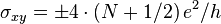 , where N is the above-mentioned integer "Landau level" index, and the double valley and double spin degeneracies give the factor of 4.[1] Moreover, in graphene these remarkable anomalies can even be measured at room temperature, i.e. at roughly 20 °C.[84] This anomalous behavior is a direct result of the emergent massless Dirac electrons in graphene. In a magnetic field, their spectrum has a Landau level with energy precisely at the Dirac point. This level is a consequence of the Atiyah–Singer index theorem and is half-filled in neutral graphene,[81] leading to the "+1/2" in the Hall conductivity.[119] Bilayer graphene also shows the quantum Hall effect, but with only one of the two anomalies (i.e.
  ). Interestingly, concerning the second anomaly, the first plateau at N = 0 is absent, indicating that bilayer graphene stays metallic at the neutrality point.[1]
, where N is the above-mentioned integer "Landau level" index, and the double valley and double spin degeneracies give the factor of 4.[1] Moreover, in graphene these remarkable anomalies can even be measured at room temperature, i.e. at roughly 20 °C.[84] This anomalous behavior is a direct result of the emergent massless Dirac electrons in graphene. In a magnetic field, their spectrum has a Landau level with energy precisely at the Dirac point. This level is a consequence of the Atiyah–Singer index theorem and is half-filled in neutral graphene,[81] leading to the "+1/2" in the Hall conductivity.[119] Bilayer graphene also shows the quantum Hall effect, but with only one of the two anomalies (i.e. ). Interestingly, concerning the second anomaly, the first plateau at N = 0 is absent, indicating that bilayer graphene stays metallic at the neutrality point.[1]
Unlike normal metals, the longitudinal resistance of graphene shows maxima rather than minima for integral values of the Landau filling factor in measurements of the Shubnikov–De Haas oscillations, which show a phase shift of π, known as Berry’s phase.[80][84] The Berry’s phase arises due to the zero effective carrier mass near the Dirac points.[120] Study of the temperature dependence of the Shubnikov–de Haas oscillations in graphene reveals that the carriers have a non-zero cyclotron mass, despite their zero effective mass from the E–k relation.[84]
[edit]Anomalous quantum Hall effect in strong magnetic fields
The quantum Hall effect in graphene in sufficiently strong magnetic fields (above 10 Teslas or so) reveals additional interesting features. Additional plateaus of the Hall conductivity at  with
with  are observed.[121] Also, the observation of a plateau at
  [122] and the fractional quantum Hall effect at
  were reported.[122][123]
with are observed.[121] Also, the observation of a plateau at [122] and the fractional quantum Hall effect at were reported.[122][123]
These observations of the quantum Hall effect with  indicate that the four-fold degeneracy (two valley and two spin degrees of freedom) of the Landau energy levels is partially or completely lifted. According to one of the suggestions, it is the magnetic catalysis of symmetry breaking that is responsible for lifting the degeneracy of the Landau levels.
indicate that the four-fold degeneracy (two valley and two spin degrees of freedom) of the Landau energy levels is partially or completely lifted. According to one of the suggestions, it is the magnetic catalysis of symmetry breaking that is responsible for lifting the degeneracy of the Landau levels.[edit]Nanostripes
Nanostripes of graphene (in the "zig-zag" orientation), at low temperatures, show spin-polarized metallic edge currents, which also suggests applications in the new field of spintronics. (In the "armchair" orientation, the edges behave like semiconductors.[124])
[edit]Graphene oxide
Further information: Graphite oxide
By dispersing oxidized and chemically processed graphite in water, and using paper-making techniques, the monolayer flakes form a single sheet and bond very powerfully. These sheets, called graphene oxide paper have a measured tensile modulus of 32 GPa.[125] The peculiar chemical property of graphite oxide is related to the functional groups attached to graphene sheets. They even can significantly change the pathway of polymerization and similar chemical processes.[126] Graphene Oxide flakes in polymers also shown enhanced photo-conducting properties.[127] A team at Manchester University led by Andre Geim published findings showing that graphene-based membranes are impermeable to all gases and liquids (vacuum-tight). However, water evaporates through them as quickly as if the membranes were not there at all.[128]
[edit]Chemical modification

Soluble fragments of graphene can be prepared in the laboratory[129] through chemical modification of graphite. First, microcrystalline graphite is treated with a strongly acidic mixture of sulfuric acid and nitric acid. A series of steps involving oxidation and exfoliation result in small graphene plates with carboxyl groups at their edges. These are converted to acid chloride groups by treatment with thionyl chloride; next, they are converted to the corresponding graphene amide via treatment with octadecylamine. The resulting material (circular graphene layers of 5.3angstrom thickness) is soluble in tetrahydrofuran, tetrachloromethane and dichloroethane. Refluxing single-layer graphene oxide (SLGO) in solvents leads to size reduction and folding of the individual sheets as well as loss of carboxylic group functionality, by up to 20%, indicating thermal instabilities of SLGO sheets dependant on their preparation methodology. When using thionyl chloride, acyl chloride groups result, which can then form aliphatic and aromatic amides with a reactivity conversion of around 70–80%.

Hydrazine reflux is commonly used for reducing SLGO to SLG(R), but titrations show that only around 20–30% of the carboxylic groups are lost leaving a significant number of COOH groups available for chemical attachment. Analysis of SLG(R) generated by this route reveals that the system is unstable and using a room temperature stirring with HCl (< 1.0 M) leads to around 60% loss of COOH functionality. Room temperature treatment of SLGO with carbodiimides leads to the collapse of the individual sheets into star-like clusters, which exhibited poor subsequent reactivity with amines (ca. 3–5% conversion of the intermediate to the final amide).[130] It is apparent that conventional chemical treatment of carboxylic groups on SLGO generates morphological changes of individual sheets that leads to a reduction in chemical reactivity, which may potentially limit their use in composite synthesis. Therefore, other types of chemical reactions have been explored. SLGO has also been grafted with polyallylamine, cross-linked through epoxy groups. When filtered into graphene oxide paper, these composites exhibit sheets increased stiffness and strength relative to unmodified graphene oxide paper.[131]
Full hydrogenation from both sides of graphene sheet results in graphane, but partial hydrogenation leads to hydrogenated graphene[132]
[edit]Thermal properties
The near-room temperature thermal conductivity of graphene was measured to be between (4.84±0.44) × 103 to (5.30±0.48) × 103 W·m−1·K−1. These measurements, made by a non-contact optical technique, are in excess of those measured for carbon nanotubes or diamond. The isotopic composition, the ratio of 12C to 13C, has a significant impact on thermal conductivity, where isotopically pure 12C graphene has higher conductivity than either a 50:50 isotope ratio or the naturally occurring 99:1 ratio.[133] It can be shown by using the Wiedemann-Franz law, that the thermal conduction is phonon-dominated.[134] However, for a gated graphene strip, an applied gate bias causing a Fermi energy shift much larger than kBT can cause the electronic contribution to increase and dominate over the phonon contribution at low temperatures. The ballistic thermal conductance of graphene is isotropic.[135][136]
Potential for this high conductivity can be seen by considering graphite, a 3D version of graphene that has basal plane thermal conductivity of over a 1,000 W·m−1·K−1 (comparable to diamond). In graphite, the c-axis (out of plane) thermal conductivity is over a factor of ~100 smaller due to the weak binding forces between basal planes as well as the larger lattice spacing.[137] In addition, the ballistic thermal conductance of a graphene is shown to give the lower limit of the ballistic thermal conductances, per unit circumference, length of carbon nanotubes.[138]
Despite its 2-D nature, graphene has 3 acoustic phonon modes. The two in-plane modes (LA, TA) have a linear dispersion relation, whereas the out of plane mode (ZA) has a quadratic dispersion relation. Due to this, the T2 dependent thermal conductivity contribution of the linear modes is dominated at low temperatures by the T1.5 contribution of the out of plane mode.[138] Some graphene phonon bands display negative Grüneisen parameters.[139] At low temperatures (where most optical modes with positive Grüneisen parameters are still not excited) the contribution from the negative Grüneisen parameters will be dominant and thermal expansion coefficient (which is directly proportional to Grüneisen parameters) negative. The lowest negative Grüneisen parameters correspond to the lowest transversal acoustic ZA modes. Phonon frequencies for such modes increase with the in-plane lattice parameter since atoms in the layer upon stretching will be less free to move in the z direction. This is similar to the behavior of a string, which, when it is stretched, will have vibrations of smaller amplitude and higher frequency. This phenomenon, named "membrane effect", was predicted by Lifshitz in 1952.[140]
[edit]Mechanical properties
As of 2009, graphene appears to be one of the strongest materials ever tested. Measurements have shown that graphene has a breaking strength over 100 times greater than a hypothetical steel film of the same (incredibly thin) thickness,[141] with a tensile modulus (stiffness) of 1 TPa (150,000,000 psi).[142] However, the process of separating it from graphite, where it occurs naturally, will require some technological development before it is economical enough to be used in industrial processes,[143] though this may be changing soon.[144] Graphene is very light, weighing only about 0.77 milligrams per square meter. The Nobel announcement illustrated this by saying that a 1 square meter graphene hammock would support a 4 kg cat but would weigh only as much as one of the cat's whiskers, at 0.77 mg about 0.001% of the weight of 1m2 of paper.[145]
Graphene paper or GP has recently been developed by a research department from the University of Technology Sydney by Guoxiu Wang, that can be processed, reshaped and reformed from its original raw material state. Researchers have successfully milled the raw graphite by purifying and filtering it with chemicals to reshape and reform it into nano-structured configurations, which are then processed into sheets as thin as paper, according to a university statement. Lead researcher Ali Reza Ranjbartoreh said: 'Not only is it lighter, stronger, harder and more flexible than steel, it is also a recyclable and sustainably manufacturable product that is eco-friendly and cost effective in its use.' Ranjbartoreh said the results would allow the development of lighter and stronger cars and planes that use less fuel, generate less pollution, are cheaper to run and ecologically sustainable. He said large aerospace companies have already started to replace metals with carbon fibres and carbon-based materials, and graphene paper with its incomparable mechanical properties would be the next material for them to explore.[citation needed]
Using an atomic force microscope (AFM), the spring constant of suspended graphene sheets has been measured. Graphene sheets, held together by van der Waals forces, were suspended over SiO2 cavities where an AFM tip was probed to test its mechanical properties. Its spring constant was in the range 1–5 N/m and the Young's modulus was0.5 TPa, which differs from that of the bulk graphite. These high values make graphene very strong and rigid. These intrinsic properties could lead to using graphene for NEMS applications such as pressure sensors and resonators.[146]
As is true of all materials, regions of graphene are subject to thermal and quantum fluctuations in relative displacement. Although the amplitude of these fluctuations is bounded in 3D structures (even in the limit of infinite size), the Mermin-Wagner theorem shows that the amplitude of long-wavelength fluctuations will grow logarithmically with the scale of a 2D structure, and would therefore be unbounded in structures of infinite size. Local deformation and elastic strain are negligibly affected by this long-range divergence in relative displacement. It is believed that a sufficiently large 2D structure, in the absence of applied lateral tension, will bend and crumple to form a fluctuating 3D structure. Researchers have observed ripples in suspended layers of graphene,[31] and it has been proposed that the ripples are caused by thermal fluctuations in the material. As a consequence of these dynamical deformations, it is debatable whether graphene is truly a 2D structure.[1][70][71][147][148]
[edit]Casimir effect and dispersion
The Casimir effect is an interaction between any disjoint neutral bodies provoked by the fluctuations of the electrodynamical vacuum. Mathematically it can be explained by considering the normal modes of electromagnetic field, which explicitly depend on the boundary (or matching) conditions on the surfaces of the interacting bodies. Since the interaction of graphene with electromagnetic field is surprisingly strong for a one-atom-thick material, the Casimir effect in the graphene systems is of growing research interest.[149][150]
The related van der Waals force (or dispersion force) is also unusual, obeying an inverse cubic asymptotic power law in contrast to the usual inverse quartic.[151]
[edit]Bilayer graphene
Main article: Bilayer graphene
Bilayer graphene is two layers of graphene and it has been shown to have interesting electrical properties, such as the quantum hall effect, a tunable band gap,[152] and potential for excitonic condensation[153] – making them promising candidates for optoelectronic and nanoelectronic applications. Bilayer graphene typically can be found either in twisted configurations where two layer are rotated relative to each other or a graphitic Bernal stacked configurations where half the atoms in one layer lie atop half the atoms in the other. Stacking order and orientation greatly influence the optical and electronic properties of bilayer graphene. One way to synthesize bilayer graphene is via chemical vapor deposition, and can produce large area bilayer regions that almost exclusively conform to a Bernal stack geometry.[154]
[edit]Potential applications
Several potential applications for graphene are under development, and many more have been proposed. These include lightweight, thin, flexible, yet durable display screens, electric circuits, and solar cells, as well as various medical, chemical and industrial processes enhanced or enabled by the use of new graphene materials.[155]
[edit]Integrated circuits
Graphene has the ideal properties to be an excellent component of integrated circuits. Graphene has a high carrier mobility, as well as low noise, allowing it to be used as the channel in a field-effect transistor. The issue is that single sheets of graphene are hard to produce, and even harder to make on top of an appropriate substrate. Researchers are looking into methods of transferring single graphene sheets from their source of origin (mechanical exfoliation on SiO2 / Si or thermal graphitization of a SiC surface) onto a target substrate of interest.[156] In 2008, the smallest transistor so far, one atom thick, 10 atoms wide was made of graphene.[157] IBM announced in December 2008 that they fabricated and characterized graphene transistors operating at GHz frequencies.[158] In May 2009, an n-type transistor was announced meaning that both n and p-type transistors have now been created with graphene.[159] A functional graphene integrated circuit was also demonstrated – a complementary inverter consisting of one p- and one n-type graphene transistor.[160] However, this inverter also suffered from a very low voltage gain.
According to a January 2010 report,[161] graphene was epitaxially grown on SiC in a quantity and with quality suitable for mass production of integrated circuits. At high temperatures, the Quantum Hall effect could be measured in these samples. See also the 2010 work by IBM in the transistor section above in which 'processors' of fast transistors on 2-inch (51 mm) graphene sheets were made.[162][163]
In June 2011, IBM researchers announced that they had succeeded in creating the first graphene-based integrated circuit, a broadband radio mixer.[164] The circuit handled frequencies up to 10 GHz, and its performance was unaffected by temperatures up to 127 degrees Celsius.
[edit]Electrochromic devices
Graphene oxide can be reversibly reduced and oxidized using electrical stimulus. Controlled reduction and oxidation in two-terminal devices containing multilayer graphene oxide films are shown to result in switching between partially reduced graphene oxide and graphene, a process that modifies the electronic and optical properties. Oxidation and reduction are also shown to be related to resistive switching.[165][166]
[edit]Transparent conducting electrodes
Graphene's high electrical conductivity and high optical transparency make it a candidate for transparent conducting electrodes, required for such applications as touchscreens, liquid crystal displays, organic photovoltaic cells, and organic light-emitting diodes. In particular, graphene's mechanical strength and flexibility are advantageous compared toindium tin oxide, which is brittle, and graphene films may be deposited from solution over large areas.[167][168]
Large-area, continuous, transparent, and highly conducting few-layered graphene films were produced by chemical vapor deposition and used as anodes for application in photovoltaic devices. A power conversion efficiency (PCE) up to 1.71% was demonstrated, which is 55.2% of the PCE of a control device based on indium-tin-oxide.[169]
Organic light-emitting diodes (OLEDs) with graphene anodes have also been demonstrated.[170] The electronic and optical performance of devices based on graphene are shown to be similar to devices made with indium-tin-oxide.
An all carbon-based device called a light-emitting electrochemical cell (LEC) was demonstrated with chemically derived graphene as the cathode and the conductive polymer PEDOT as the anode by Matyba et al.[171] Unlike its predecessors, this device contains no metal, but only carbon-based electrodes. The use of graphene as the anode in LECs was also verified in the same publication.
[edit]Room temperature distillation of ethanol for fuel and human consumption
Graphene oxide membranes will allow water vapor to pass through, but have been shown to be impermeable to all other liquids and gases including helium .[128] This phenomenon has been used for further distilling of vodka to higher alcohol concentrations, in a room-temperature laboratory, without the application of heat or vacuum normally used in traditional distillation methods.[172] Further development and commercialization of such membranes could revolutionize the economics of biofuel production and the alcoholic beverage industry.
[edit]Desalination
Research suggests that graphene filters could outperform other techniques of desalination by a significant margin.[173][174]
[edit]Solar cells
The USC Viterbi School of Engineering lab reported the large scale production of highly transparent graphene films by chemical vapor deposition in 2008. In this process, researchers create ultra-thin graphene sheets by first depositing carbon atoms in the form of graphene films on a nickel plate from methane gas. Then they lay down a protective layer of thermoplastic over the graphene layer and dissolve the nickel underneath in an acid bath. In the final step they attach the plastic-protected graphene to a very flexible polymer sheet, which can then be incorporated into an OPV cell (graphene photovoltaics). Graphene/polymer sheets have been produced that range in size up to 150 square centimeters and can be used to create dense arrays of flexible OPV cells. It may eventually be possible to run printing presses laying extensive areas covered with inexpensive solar cells, much like newspaper presses print newspapers (roll-to-roll).[175][176]
While silicon has long been the standard for commercial solar cells, new research from the Institute of Photonic Sciences (ICFO) in Spain has shown that graphene could prove far more efficient when it comes to transforming light into energy. The study found that unlike silicon, which generates only one current-driving electron for each photon it absorbs, graphene can produce multiple electrons. Solar cells made with graphene could offer 60% solar cell efficiency – double the widely-regarded maximum efficiency of silicon cells.[177]
[edit]Single-molecule gas detection
Theoretically graphene makes an excellent sensor due to its 2D structure. The fact that its entire volume is exposed to its surrounding makes it very efficient to detect adsorbed molecules. However, similar to carbon nanotubes, graphene has no dangling bonds on its surface. Gaseous molecules cannot be readily adsorbed onto graphene surface. So intrinsically graphene is insensitive.[178] The sensitivity of graphene chemical gas sensors can be dramatically enhanced by functionalizing graphene, for example, coating with a thin layer of certain polymers. The thin polymer layer acts like a concentrator that absorbs gaseous molecules. The molecule absorption introduces a local change inelectrical resistance of graphene sensors. While this effect occurs in other materials, graphene is superior due to its high electrical conductivity (even when few carriers are present) and low noise, which makes this change in resistance detectable.[90]
[edit]Graphene nanoribbons
Graphene nanoribbons (GNRs) are essentially single layers of graphene that are cut in a particular pattern to give them certain electrical properties. Depending on how the un-bonded edges are configured, they can either be in a zigzag or armchair configuration. Calculations based on tight binding predict that zigzag GNRs are always metallic while armchairs can be either metallic or semiconducting, depending on their width. However, recent density functional theory calculations show that armchair nanoribbons are semiconducting with an energy gap scaling with the inverse of the GNR width.[179] Indeed, experimental results show that the energy gaps do increase with decreasing GNR width.[180] However, as of February 2008, no experimental results have measured the energy gap of a GNR and identified the exact edge structure. Zigzag nanoribbons are also semiconducting and present spin-polarized edges. Their 2D structure, high electrical and thermal conductivity, and low noise also make GNRs a possible alternative to copper for integrated circuit interconnects. Some research is also being done to create quantum dots by changing the width of GNRs at select points along the ribbon, creating quantum confinement.[181] Large quantities of width controlled GNRs can be produced via graphite nanotomy process.[182]
[edit]Graphene quantum dots
Graphene quantum dots (GQDs) are single atom thick sheets of graphene with all dimensions less than 100 nm. Their size and edge crystallography govern their electrical, magnetic, optical and chemical properties. GQDs can be produced via graphite nanotomy as shown by Berry group[182] or via bottom-up, solution-based routes (Diels-Alder, cyclotrimerization and/or cyclodehydrogenation reactions) shown by Mullen group.[183] Several studies[157] have indicated that GQDs with controlled structure can be incorporated into a wide variety of applications in electronics, optoelectronics and electromagnetics.
[edit]Graphene transistors
Due to its high electronic quality, graphene has also attracted the interest of technologists who see it as a way of constructing ballistic transistors. Graphene exhibits a pronounced response to perpendicular external electric fields, allowing one to build FETs (field-effect transistors). In their 2004 paper,[15] the Manchester group demonstrated FETs with a "rather modest" on-off ratio of ~30 at room temperature. In 2006, Georgia Tech researchers, led by Walter de Heer, announced that they had successfully built an all-graphene planar FET with side gates.[184] Their devices showed changes of 2% at cryogenic temperatures. The first top-gated FET (on–off ratio of <2 a="" by="" class="new" demonstrated="" href="http://en.wikipedia.org/w/index.php?title=AMICA&action=edit&redlink=1" nbsp="" of="" researchers="" style="background-image: none; background-position: initial initial; background-repeat: initial initial; color: #a55858; text-decoration: none;" title="AMICA (page does not exist)" was="">AMICA
Facing the fact that current graphene transistors show a very poor on–off ratio, researchers are trying to find ways for improvement. In 2008, researchers of AMICA and University of Manchester demonstrated a new switching effect in graphene field-effect devices. This switching effect is based on a reversible chemical modification of the graphene layer and gives an on–off ratio of greater than six orders of magnitude. These reversible switches could potentially be applied to nonvolatile memories.[187]
In 2009, researchers at the Politecnico di Milano demonstrated four different types of logic gates, each composed of a single graphene transistor.[188] In the same year, the Massachusetts Institute of Technology researchers built an experimental graphene chip known as a frequency multiplier. It is capable of taking an incoming electrical signal of a certain frequency and producing an output signal that is a multiple of that frequency.[189] Similar results are obtained in.[190] Although these graphene chips open up a range of new applications, their practical use is limited by a very small voltage gain (typically, the amplitude of the output signal is about 40 times less than that of the input signal). Moreover, none of these circuits was demonstrated to operate at frequencies higher than 25 kHz. In the same year, tight-binding numerical simulations[191] obtained by means of the open-source software NanoTCAD ViDES have demonstrated that the band-gap induced in graphene bilayer field effect transistors is not sufficiently large for high-performance transistors for digital applications, but it can be sufficient for ultra-low voltage applications, when exploiting a tunnel-FET architecture.[192]
In February 2010, researchers at IBM reported that they have been able to create graphene transistors with an on and off rate of 100 gigahertz, far exceeding the rates of previous attempts, and exceeding the speed of silicon transistors with an equal gate length. The 240 nm graphene transistors made at IBM were made using extant silicon-manufacturing equipment, meaning that for the first time graphene transistors are a conceivable – though still fanciful – replacement for silicon.[162][163][193]
In November 2011, researchers at Cambridge University demonstrated the feasibility of ink-jet printing as a method for fabricating graphene devices.[194]
In 2013, researchers at the Tokyo Institute of Technology have exploited graphene's high mobility in a novel detector that allows broad band frequency selectivity ranging from the THz to IR region (0.76-33THz)[195]
[edit]Graphene optical modulators
When the Fermi level of graphene is tuned, the optical absorption of graphene can be changed. In 2011, researchers at UC Berkeley reported the first graphene-based optical modulator. Operating at 1.2 GHz without any temperature controller, this modulator has a broad bandwidth (from 1.3 to 1.6 μm) and small footprint (~25 μm2).[196]
[edit]Reference material for characterizing electroconductive and transparent materials
One layer of graphene absorbs 2.3% of white light.[197] This property was used to define the conductivity of transparency that combines the sheet resistance and the transparency. This parameter was used to compare different materials without the use of two independent parameters.[198]
[edit]Thermal management materials
In 2011, researchers in Georgia Institute of Technology reported that a three-dimensional vertically aligned functionalized multilayer graphene architecture can be an approach for graphene-based thermal interfacial materials (TIMs) with superior equivalent thermal conductivity and ultra-low interfacial thermal resistance between graphene and metal.[136]
[edit]Ultracapacitors
Due to the extremely high surface area to mass ratio of graphene, one potential application is in the conductive plates of ultracapacitors. It is believed that graphene could be used to produce ultracapacitors with a greater energy storage density than is currently available.[199]
[edit]Engineered piezoelectricity
Density functional theory simulations predict that depositing certain adatoms on graphene can render it piezoelectrically responsive to an electric field applied in the vertical (i.e. out-of-plane) direction. This type of locally engineered piezoelectricity is similar in magnitude to that of bulk piezoelectric materials and make graphene a candidate tool for control and sensing in nanoscale devices.[200][201]
[edit]Graphene biodevices
Graphene's modifiable chemistry, large surface area, atomic thickness and molecularly gatable structure make antibody-functionalized graphene sheets excellent candidates for mammalian and microbial detection and diagnosis devices.[202]

The most ambitious biological application of graphene is for rapid, inexpensive electronic DNA sequencing. Integration of graphene (thickness of 0.34 nm) layers as nanoelectrodes into a nanopore[203] can solve one of the bottleneck issues of nanopore-based single-molecule DNA sequencing.
[edit]Pseudo-relativistic theory
The electrical properties of graphene can be described by a conventional tight-binding model; in this model the energy of the electrons with wave vector k is[79][81]

with the nearest-neighbor hopping energy γ0 ≈ 2.8 eV and the lattice constant a ≈ 2.46 Å. Conduction and valence band, respectively, correspond to the different signs in the above dispersion relation; they touch each other in six points, the "K-values". However, only two of these six points are independent, whereas the rest is equivalent by symmetry. In the vicinity of the K-points the energy depends linearly on the wave vector, similar to a relativistic particle. Since an elementary cell of the lattice has a basis of two atoms, the wave function even has an effective 2-spinor structure. As a consequence, at low energies, even neglecting the true spin, the electrons can be described by an equation that is formally equivalent to the massless Dirac equation. Moreover, in the present case this pseudo-relativistic description is restricted to the chiral limit, i.e., to vanishing rest mass M0, which leads to interesting additional features:[81][204]

Here vF ~ 106 is the Fermi velocity in graphene, which replaces the velocity of light in the Dirac theory;  is the vector of the Pauli matrices,
  is the two-component wave function of the electrons, and E is their energy.[124]
is the vector of the Pauli matrices, is the two-component wave function of the electrons, and E is their energy.[124][edit]History and experimental discovery
The term graphene first appeared in 1987[205] to describe single sheets of graphite as one of the constituents of graphite intercalation compounds (GICs); conceptually a GIC is a crystalline salt of the intercalant and graphene. The term was also used in early descriptions of carbon nanotubes,[206] as well as for epitaxial graphene,[207] and polycyclic aromatic hydrocarbons.[208]
Larger graphene molecules or sheets (so that they can be considered as true isolated 2D crystals) cannot be grown even in principle. An article in Physics Today reads:
Fundamental forces place seemingly insurmountable barriers in the way of creating [2D crystals]... The nascent 2D crystallites try to minimize their surface energy and inevitably morph into one of the rich variety of stable 3D structures that occur in soot. But there is a way around the problem. Interactions with 3D structures stabilize 2D crystals during growth. So one can make 2D crystals sandwiched between or placed on top of the atomic planes of a bulk crystal. In that respect, graphene already exists within graphite... One can then hope to fool Nature and extract single-atom-thick crystallites at a low enough temperature that they remain in the quenched state prescribed by the original higher-temperature 3D growth.[30]
Single layers of graphite were previously (starting from the 1970s) grown epitaxially on top of other materials.[209] This "epitaxial graphene" consists of a single-atom-thick hexagonal lattice of sp2-bonded carbon atoms, as in free-standing graphene. However, there is significant charge transfer from the substrate to the epitaxial graphene, and, in some cases, hybridization between the d orbitals of the substrate atoms and π orbitals of graphene, which significantly alters the electronic structure of the epitaxial graphene.
Single layers of graphite were also observed by transmission electron microscopy within bulk materials (see section Occurrence), in particular inside soot obtained by chemical exfoliation.[14] There have also been a number of efforts to make very thin films of graphite by mechanical exfoliation (starting from 1990 and continuing until after 2004)[14] but nothing thinner than 50 to 100 layers was produced during these years.

A key advance in the science of graphene came when Andre Geim and Kostya Novoselov at Manchester University managed to extract single-atom-thick crystallites (graphene) from bulk graphite in 2004.[15] The Manchester researchers pulled out graphene layers from graphite and transferred them onto thin SiO2 on a silicon wafer in a process sometimes called micromechanical cleavage or, simply, the Scotch tape technique. The SiO2 electrically isolated the graphene, and was weakly interacting with the graphene, providing nearly charge-neutral graphene layers. The silicon beneath the SiO2 could be used as a "back gate" electrode to vary the charge density in the graphene layer over a wide range.
The micromechanical cleavage technique led directly to the first observation of the anomalous quantum Hall effect in graphene,[84][120] which provided direct evidence of the theoretically predicted pi Berry's phase of massless Dirac fermions in graphene. The anomalous quantum Hall effect in graphene was reported around the same time by Geim and Novoselov and by Philip Kim and Yuanbo Zhang in 2005. These simple experiments started after the researchers watched colleagues who were looking for quantum Hall effect[210] and Dirac fermions[211] in bulk graphite.
Geim has received several awards for his pioneering research on graphene, including the 2007 Mott medal for the "discovery of a new class of materials – free-standing two-dimensional crystals – in particular graphene", the 2008 EuroPhysics Prize (together with Novoselov) "for discovering and isolating a single free-standing atomic layer of carbon (graphene) and elucidating its remarkable electronic properties", and the 2009 Körber Prize for "develop[ing] the first two-dimensional crystals made of carbon atoms". In 2008 and 2009, Reuters tipped him as one of the front-runners for a Nobel prize in Physics.[212]On October 5, 2010, the Nobel Prize in Physics for the year was awarded to Andre Geim and Konstantin Novoselov from the University of Manchester for their work on graphene.[213]
The theory of graphene was first explored by P. R. Wallace in 1947 as a starting point for understanding the electronic properties of more complex, 3D graphite. The emergent massless Dirac equation was first pointed out by Gordon Walter Semenoff and David P. DeVincenzo and Eugene J. Mele.[214]Semenoff emphasized the occurrence in a magnetic field of an electronic Landau level precisely at the Dirac point. This level is responsible for the anomalous integer quantum Hall effect.[84][119][120] Later, single graphene layers were also observed directly by electron microscopy.[31]
More recently, graphene samples prepared on nickel films, and on both the silicon face and carbon face of silicon carbide, have shown the anomalous quantum Hall effect directly in electrical measurements.[38][39][40][41][42] Graphitic layers on the carbon face of silicon carbide show a clear Dirac spectrum inangle-resolved photoemission experiments, and the anomalous quantum Hall effect is observed in cyclotron resonance and tunneling experiments.[215] Even though graphene on nickel and on silicon carbide have both existed in the laboratory for decades, it was graphene mechanically exfoliated on SiO2 that provided the first proof of the Dirac fermion nature of electrons in graphene.[citation needed]
[edit]See also
[edit]References
- ^ a b c d e f g h i j Geim, A. K. and Novoselov, K. S. (2007). "The rise of graphene". Nature Materials 6 (3): 183–191.Bibcode:2007NatMa...6..183G. doi:10.1038/nmat1849.PMID 17330084.
- ^ a b H. P. Boehm, R. Setton, E. Stumpp (1994). "Nomenclature and terminology of graphite intercalation compounds". Pure and Applied Chemistry 66 (9): 1893–1901.doi:10.1351/pac199466091893.
- ^ H. P. Boehm, A. Clauss, G. O. Fischer, U. Hofmann (1962). "Das Adsorptionsverhalten sehr dünner Kohlenstoffolien". Zeitschrift für anorganische und allgemeine Chemie 316 (3–4): 119–127.doi:10.1002/zaac.19623160303.
- ^ Raji Heyrovska (2008). "Atomic Structures of Graphene, Benzene and Methane with Bond Lengths as Sums of the Single, Double and Resonance Bond Radii of Carbon".arXiv:0804.4086 [physics.gen-ph].
- ^ Nobel Foundation announcement
- ^ http://europa.eu/rapid/press-release_IP-13-54_en.htm
- ^ "graphene layer". IUPAC Gold Book. International Union of Pure and Applied Chemistry. Retrieved 31 March 2012.
- ^ Simpson, C. D. et al. (2002). "Synthesis of a Giant 222 Carbon Graphite Sheet". Chemistry – A European Journal 6 (6): 1424.doi:10.1002/1521-3765(20020315)8:6<1424::aid-chem1424>3.0.CO;2-Z.
- ^ a b Sakamoto J. et al (2009). "Two-Dimensional Polymers: Just a Dream of Synthetic Chemists?". Angew. Chem. Int. Ed. 48 (16): 1030–69. doi:10.1002/anie.200801863. PMID 19130514.
- ^ a b O. B. Shenderova, V. V. Zhirnov, D. W. Brenner (2002). "Carbon Nanostructures". Critical Reviews in Solid State and Materials Sciences 27 (3–4): 227.Bibcode:2002CRSSM..27..227S.doi:10.1080/10408430208500497.
- ^ S. Braga, V. R. Coluci, S. B. Legoas, R. Giro, D. S. Galvão, R. H. Baughman (2004). "Structure and Dynamics of Carbon Nanoscrolls". Nano Letters 4 (5): 881.Bibcode:2004NanoL...4..881B. doi:10.1021/nl0497272.
- ^ Geim A. (2009). "Graphene: Status and Prospects". Science 324(5934): 1530–4. Bibcode:2009Sci...324.1530G.doi:10.1126/science.1158877. PMID 19541989.
- ^ a b Riedl C., Coletti C., Iwasaki T., Zakharov A.A., Starke U. (2009). "Quasi-Free-Standing Epitaxial Graphene on SiC Obtained by Hydrogen Intercalation". Phys. Rev. Lett. 103 (24): 246804.Bibcode:2009PhRvL.103x6804R.doi:10.1103/PhysRevLett.103.246804. PMID 20366220.
- ^ a b c d e "Carbon Wonderland". Scientific American. April 2008. Retrieved 2009-05-05. ".. bits of graphene are undoubtedly present in every pencil mark"
- ^ a b c d e Novoselov, K. S. et al. (2004). "Electric Field Effect in Atomically Thin Carbon Films". Science 306 (5696): 666–9.arXiv:cond-mat/0410550. Bibcode:2004Sci...306..666N.doi:10.1126/science.1102896. PMID 15499015.
- ^ a b H.P. Boehm, A. Clauss, G. Fischer, U. Hofmann (1962). "Surface Properties of Extremely Thin Graphite Lamellae".Proceedings of the Fifth Conference on Carbon by Pergamon Press. N.B. This paper reports graphitic flakes that give an additional contrast equivalent of down to ~4A or 3 atomic layers of amorphous carbon. This was the best possible resolution for 1960 TEMs. However, neither then nor today it is possible to argue how many layers were in those flakes. Now we know that the TEM contrast of graphene most strongly depends on focusing conditions [Meyer et al, Nature 446, 60 (2007)]. For example, it is impossible to distinguish between suspended monolayer and multilayer graphene by their TEM contrasts, and the only known way is to analyse relative intensities of various diffraction spots. The first reliable TEM observations of monolayers are probably given in refs. 24 and 26 of Geim & Novoselov, Nature Materials 6, 183 (2007).
- ^ G. Ruess and F. Vogt (1948). "Höchstlamellarer Kohlenstoff aus Graphitoxyhydroxyd". Monatshefte für Chemie 78 (3–4): 222–242.doi:10.1007/BF01141527.
- ^ Brodie, B. C. "On the Atomic Weight of Graphite". Philos. Trans. R. Soc. London 1859, 14, 249–259.
- ^ V. Kohlschütter and P. Haenni (1918). "Zur Kenntnis des Graphitischen Kohlenstoffs und der Graphitsäure". Z. Anorg. Allg. Chem. 105 (1): 121–144. doi:10.1002/zaac.19191050109.
- ^ October 22, 2004: Discovery of Graphenehttp://www.aps.org/publications/apsnews/200910/physicshistory.cfm
- ^ Vorbeck Materials. "Realizing graphene's possibilities".
- ^ Segal, Michael (2009). "Selling graphene by the ton". Nature Nanotechnology 4 (10): 612–4. Bibcode:2009NatNa...4..612S.doi:10.1038/nnano.2009.279. PMID 19809441.
- ^ Graphene Commercialisation & Applications 2013: Global Industry & Academia Collaboration Summit
- ^ Patel, Prachi, "Bigger, Stretchier Graphene", Technology Review, MIT, 2009-01-15
- ^ a b c Bae, S. et al. (2010). "Roll-to-roll production of 30-inch graphene films for transparent electrodes". Nature nanotechnology5 (8): 574–8. Bibcode:2010NatNa...5..574B.doi:10.1038/nnano.2010.132. PMID 20562870.
- ^ Polish scientists to patent graphene mass-production technology | Graphene Times
- ^ Polish team claims leap for wonder material graphene
- ^ Gall,N.R.; Rut’kov, E.V.; Tontegode, A.Y. (1997). "Two Dimensional Graphite Films on Metals and Their Intercalation".International Journal of Modern Physics B 11 (16): 1865–1911.Bibcode:1997IJMPB..11.1865G.doi:10.1142/S0217979297000976.
- ^ Gall,N.R.; Rut’kov, E.V.; Tontegode, A.Y. (1995). "Influence of surface carbon on the formation of silicon-refractory metal interfaces". Thin Solid Films 266 (2): 229–233.Bibcode:1995TSF...266..229G. doi:10.1016/0040-6090(95)06572-5.
- ^ a b Geim, A. K. & MacDonald, A. H. (2007). "Graphene: Exploring carbon flatland". Physics Today 60 (8): 35–41.Bibcode:2007PhT....60h..35G.doi:10.1063/1.2774096.[dead link]
- ^ a b c d Meyer, J. et al. (2007). "The structure of suspended graphene sheets". Nature 446 (7131): 60–63. arXiv:cond-mat/0701379. Bibcode:2007Natur.446...60M.doi:10.1038/nature05545. PMID 17330039.
- ^ Novoselov, K.S. et al. (2005). "Two-dimensional atomic crystals". PNAS 102 (30): 10451–3. arXiv:cond-mat/0503533. Bibcode:2005PNAS..10210451N.doi:10.1073/pnas.0502848102. PMC 1180777.PMID 16027370.
- ^ Sutter, P. (2009). "Epitaxial graphene: How silicon leaves the scene". Nature Materials 8 (3): 171–2.Bibcode:2009NatMa...8..171S. doi:10.1038/nmat2392.PMID 19229263.
- ^ a b Ohta, T. et al. (2007). "Interlayer Interaction and Electronic Screening in Multilayer Graphene Investigated with Angle-Resolved Photoemission Spectroscopy". Physical Review Letters98 (20): 206802. Bibcode:2007PhRvL..98t6802O.doi:10.1103/PhysRevLett.98.206802. PMID 17677726.
- ^ a b Bostwick, A. et al. (2007). "Symmetry breaking in few layer graphene films". New Journal of Physics 9 (10): 385.Bibcode:2007NJPh....9..385B. doi:10.1088/1367-2630/9/10/385.
- ^ Zhou, S.Y. et al. (2006). "First direct observation of Dirac fermions in graphite". Nature Physics 2 (9): 595–599. arXiv:cond-mat/0608069. Bibcode:2006NatPh...2..595Z.doi:10.1038/nphys393.
- ^ Morozov, S.V. et al. (2006). "Strong Suppression of Weak Localization in Graphene". Physical Review Letters 97 (1): 016801. arXiv:cond-mat/0603826.Bibcode:2006PhRvL..97a6801M.doi:10.1103/PhysRevLett.97.016801. PMID 16907394.
- ^ a b c Kim, Kuen Soo; et al. (2009). "Large-scale pattern growth of graphene films for stretchable transparent electrodes". Nature 457(7230): 706–10. Bibcode:2009Natur.457..706K.doi:10.1038/nature07719. PMID 19145232.
- ^ a b Johannes Jobst, Daniel Waldmann, Florian Speck, Roland Hirner, Duncan K. Maude, Thomas Seyller, Heiko B. Weber (2009). "How Graphene-like is Epitaxial Graphene? Quantum Oscillations and Quantum Hall Effect". arXiv:0908.1900 [cond-mat.mes-hall].
- ^ a b T. Shen, J.J. Gu, M. Xu, Y.Q. Wu, M.L. Bolen, M.A. Capano, L.W. Engel, P.D. Ye (2009). "Observation of quantum-Hall effect in gated epitaxial graphene grown on SiC (0001)". Applied Physics Letters 95 (17): 172105. Bibcode:2009ApPhL..95q2105S.doi:10.1063/1.3254329.
- ^ a b Xiaosong Wu, Yike Hu, Ming Ruan, Nerasoa K Madiomanana, John Hankinson, Mike Sprinkle, Claire Berger, Walt A. de Heer (2009). "Half integer quantum Hall effect in high mobility single layer epitaxial graphene". Applied Physics Letters95 (22): 223108. arXiv:0909.2903. doi:10.1063/1.3266524.
- ^ a b Samuel Lara-Avila, Alexei Kalaboukhov, Sara Paolillo, Mikael Syväjärvi, Rositza Yakimova, Vladimir Fal'ko, Alexander Tzalenchuk, Sergey Kubatkin (2009). "SiC Graphene Suitable For Quantum Hall Resistance Metrology". Nature Nanotechnology 5(3): 186–9. arXiv:0909.1193. doi:10.1038/nnano.2009.474.PMID 20081845.
- ^ a b Hass, J. et al. (2008). "Why multilayer graphene on 4H-SiC(000(1)over-bar) behaves like a single sheet of graphene".Physical Review Letters 100 (12): 125504.Bibcode:2008PhRvL.100l5504H.doi:10.1103/PhysRevLett.100.125504.
- ^ Berger, C. et al. (2004). "Ultrathin epitaxial graphite: 2D electron gas properties and a route toward graphene-based nanoelectronics". Journal of Physical Chemistry B 108 (52): 19912–19916. doi:10.1021/jp040650f.
- ^ Patterned thin film graphite devices and method for making same US Patent 7015142
- ^ Kedzierski, J. et al. (2008). "Epitaxial Graphene Transistors on SiC Substrates". IEEE Transactions on Electron Devices 55 (8): 2078–2085. Bibcode:2008ITED...55.2078K.doi:10.1109/TED.2008.926593.
- ^ Moon, J.S. et al. (2009). "Epitaxial-Graphene RF Field-Effect Transistors on Si-Face 6H-SiC Substrates". IEEE Electron Device Letters 30 (6): 650–652. Bibcode:2009IEDL...30..650M.doi:10.1109/LED.2009.2020699.
- ^ Singh, Ram Sevak; Nalla, Venkatram; Chen, Wei; Wee, Andrew Thye Shen; Ji, Wei (2011). "Laser Patterning of Epitaxial Graphene for Schottky Junction Photodetectors". ACS Nano 5 (7): 5969–75.doi:10.1021/nn201757j. PMID 21702443.
- ^ "A smarter way to grow graphene". PhysOrg.com. May 2008.
- ^ Pletikosić, I. et al. (2009). "Dirac Cones and Minigaps for Graphene on Ir(111)". Physical Review Letters 102 (5): 056808.Bibcode:2009PhRvL.102e6808P.doi:10.1103/PhysRevLett.102.056808.
- ^ Li, Xuesong; et al. (2009). "Large-Area Synthesis of High-Quality and Uniform Graphene Films on Copper Foils". Science 324(5932): 1312–4. Bibcode:2009Sci...324.1312L.doi:10.1126/science.1171245. PMID 19423775.
- ^ Wassei, Jonathan K.; Mecklenburg, Matthew; Torres, Jaime A.; Fowler, Jesse D.; Regan, B. C.; Kaner, Richard B.; Weiller, Bruce H. (12). "Chemical Vapor Deposition of Graphene on Copper from Methane, Ethane and Propane: Evidence for Bilayer Selectivity".Small 8 (9): 1415–1422. doi:10.1002/smll.201102276.PMID 22351509.
- ^ Lenski, Daniel R.; Fuhrer, Michael S. (2011). "Raman and optical characterization of multilayer turbostratic graphene grown via chemical vapor deposition". Journal of Applied Physics 110: 013720. doi:10.1063/1.3605545.
- ^ Weatherup, R.S. et al. (2011). "In Situ Characterization of Alloy Catalysts for Low-Temperature Graphene Growth". Nano Letters11 (10): 4154–60. doi:10.1021/nl202036y. PMID 21905732.
- ^ Boehm’s 1961 isolation of graphene. Graphene Times (2009-12-07). Retrieved on 2010-12-10.
- ^ Eswaraiah, Varrla et al. "Top down method for synthesis of highly conducting graphene by exfoliation of graphite oxide using focused solar radiation". Graphene synthesis. Royal Society of Chemistry. Retrieved 6 April 2011. More than one of
|author=and|last=specified (help) - ^ Ji, Liwen et al. "SnS2 nanoparticle loaded graphene nanocomposites for superior energy storage". Royal Society of Chemistry. Retrieved March 2012. More than one of
|author=and|last=specified (help) - ^ http://www.sciencemag.org/content/335/6074/1326
- ^ http://newsroom.ucla.edu/portal/ucla/ucla-researchers-develop-new-graphene-230478.aspx
- ^ http://newsroom.ucla.edu/portal/ucla/ucla-researchers-develop-new-technique-243553.aspx
- ^ a b Shaahin Amini, Javier Garay, Guanxiong Liu, Alexander A. Balandin, Reza Abbaschian (2010). "Growth of Large-Area Graphene Films from Metal-Carbon Melts". Journal of Applied Physics 108 (9): 094321. Bibcode:2010JAP...108i4321A.doi:10.1063/1.3498815.
- ^ Choucair, M.; Thordarson, P; Stride, JA (2008). "Gram-scale production of graphene based on solvothermal synthesis and sonication". Nature Nanotechnology 4 (1): 30–3.Bibcode:2009NatNa...4...30C. doi:10.1038/nnano.2008.365.PMID 19119279.
- ^ Brumfiel, G. (2009). "Nanotubes cut to ribbons New techniques open up carbon tubes to create ribbons". Nature.doi:10.1038/news.2009.367.
- ^ Kosynkin, D. V. et al. (2009). "Longitudinal unzipping of carbon nanotubes to form graphene nanoribbons". Nature 458 (7240): 872–6. Bibcode:2009Natur.458..872K.doi:10.1038/nature07872. PMID 19370030.
- ^ Liying Jiao, Li Zhang, Xinran Wang, Georgi Diankov & Hongjie Dai (2009). "Narrow graphene nanoribbons from carbon nanotubes". Nature 458 (7240): 877–80.Bibcode:2009Natur.458..877J. doi:10.1038/nature07919.PMID 19370031.
- ^ High-yield production of graphene by liquid-phase exfoliation of graphite : Abstract : Nature Nanotechnology
- ^ Graphene-containing thermoresponsive nanocomposite hydrogels of poly(N-isopropylacrylamide) prepared by frontal polymerization – Journal of Materials Chemistry (RSC Publishing)
- ^ High concentration few-layer graphene sheets obtained by liquid phase exfoliation of graphite in ionic liquid – Journal of Materials Chemistry (RSC Publishing)
- ^ Chakrabarti, A; Lu, J.; Skrabutenas, J. C.; Xu, T.; Xiao, Z.; Maguire, J. A.; Hosmane, N. S. (2011). "Conversion of carbon dioxide to few-layer graphene". Journal of Materials Chemistry 21(26): 9491–9493. doi:10.1039/C1JM11227A.
- ^ a b Carlsson, J. M. (2007). "Graphene: Buckle or break". Nature Materials 6 (11): 801–2. Bibcode:2007NatMa...6..801C.doi:10.1038/nmat2051. PMID 17972931.
- ^ a b Fasolino, A., Los, J. H., & Katsnelson, M. I. (2007). "Intrinsic ripples in graphene". Nature Materials 6 (11): 858–61.Bibcode:2007NatMa...6..858F. doi:10.1038/nmat2011.PMID 17891144.
- ^ a b c Ishigami, Masa; et al. (2007). "Atomic Structure of Graphene on SiO2". Nano Lett 7 (6): 1643–1648.Bibcode:2007NanoL...7.1643I. doi:10.1021/nl070613a.PMID 17497819.
- ^ Stolyarova, Elena; et al. (2007). "High-resolution scanning tunneling microscopy imaging of mesoscopic graphene sheets on an insulating surface". Proceedings of the National Academy of Sciences 104 (22): 9209–9212.Bibcode:2007PNAS..104.9209S.doi:10.1073/pnas.0703337104. PMC 1874226.PMID 17517635.
- ^ Kasuya, D.; Yudasaka, M.; Takahashi, K.; Kokai, F.; Iijima, S. (2002). "Selective Production of Single-Wall Carbon Nanohorn Aggregates and Their Formation Mechanism". J. Phys. Chem. B106 (19): 4947. doi:10.1021/jp020387n.
- ^ Bernatowicz, T. J. et al. (1996). "Constraints on stellar grain formation from presolar graphite in the Murchison meteorite".Astrophysical Journal 472 (2): 760–782.Bibcode:1996ApJ...472..760B. doi:10.1086/178105.
- ^ Fraundorf, P. and Wackenhut, M. (2002). "The core structure of presolar graphite onions". Astrophysical Journal Letters 578 (2): L153–156. arXiv:astro-ph/0110585.Bibcode:2002ApJ...578L.153F. doi:10.1086/344633.
- ^ Recep Zan, Quentin M. Ramasse, Ursel Bangert, Konstantin S. Novoselov (2012). "Graphene re-knits its holes". Mesoscale and Nanoscale Physics. arXiv:1207.1487v1.
- ^ Graphene sheets can repair themselves naturallyhttp://www.zmescience.com/research/studies/graphene-can-repair-self-automatically-12072012/
- ^ a b Wallace, P. R. (1947). "The Band Theory of Graphite".Physical Review 71 (9): 622. Bibcode:1947PhRv...71..622W.doi:10.1103/PhysRev.71.622.
- ^ a b c d Charlier, J.-C.; Eklund, P.C.; Zhu, J. and Ferrari, A.C. (2008). "Electron and Phonon Properties of Graphene: Their Relationship with Carbon Nanotubes". from Carbon Nanotubes: Advanced Topics in the Synthesis, Structure, Properties and Applications, Ed. A. Jorio, G. Dresselhaus, and M.S. Dresselhaus. Berlin/Heidelberg: Springer-Verlag.
- ^ a b c d e Semenoff, G. W. (1984). "Condensed-Matter Simulation of a Three-Dimensional Anomaly". Physical Review Letters 53(26): 2449. Bibcode:1984PhRvL..53.2449S.doi:10.1103/PhysRevLett.53.2449.
- ^ a b Avouris, P., Chen, Z., and Perebeinos, V. (2007). "Carbon-based electronics". Nature Nanotechnology 2 (10): 605–15.Bibcode:2007NatNa...2..605A. doi:10.1038/nnano.2007.300.PMID 18654384.
- ^ Hernández, Saúl; Raya, Alfredo (January 2012). "Hard and soft supersymmetry breaking for 'graphinos' in uniform magnetic fields". Journal of Physics: Condensed Matter 24 (1): (5pp).doi:10.1088/0953-8984/24/1/015304. PMID 22156191.
- ^ a b c d e f Novoselov, K. S. et al. (2005). "Two-dimensional gas of massless Dirac fermions in graphene". Nature 438 (7065): 197–200. arXiv:cond-mat/0509330.Bibcode:2005Natur.438..197N. doi:10.1038/nature04233.PMID 16281030.
- ^ Morozov, S.V. et al. (2008). "Giant Intrinsic Carrier Mobilities in Graphene and Its Bilayer". Phys. Rev. Lett 100 (1): 016602.Bibcode:2008PhRvL.100a6602M.doi:10.1103/PhysRevLett.100.016602. PMID 18232798.
- ^ a b c Chen, J. H. et al. (2008). "Intrinsic and Extrinsic Performance Limits of Graphene Devices on SiO2". Nature Nanotechnology 3 (4): 206–9. doi:10.1038/nnano.2008.58.PMID 18654504.
- ^ Akturk, A. and Goldsman, N. (2008). "Electron transport and full-band electron–phonon interactions in graphene". Journal of Applied Physics 103 (5): 053702.Bibcode:2008JAP...103e3702A. doi:10.1063/1.2890147.
- ^ Physicists Show Electrons Can Travel More Than 100 Times Faster in Graphene
- ^ a b c Chen, J. H. et al. (2008). "Charged Impurity Scattering in Graphene". Nature Physics 4 (5): 377–381.Bibcode:2008NatPh...4..377C. doi:10.1038/nphys935.
- ^ a b c Schedin, F. et al. (2007). "Detection of individual gas molecules adsorbed on graphene". Nature Mater 6 (9): 652–655.Bibcode:2007NatMa...6..652S. doi:10.1038/nmat1967.PMID 17660825.
- ^ Adam, S. et al. (2007). "A self-consistent theory for graphene transport". Proc. Nat. Acad. Sci. USA 104 (47): 18392–7.arXiv:0705.1540. Bibcode:2007PNAS..10418392A.doi:10.1073/pnas.0704772104. PMC 2141788.PMID 18003926.
- ^ Hadar Steinberg, Gilad Barak, Amir Yacoby, et al (2008). "Charge fractionalization in quantum wires (Letter)". Nature Physics 4 (2): 116–119. Bibcode:2008NatPh...4..116S.doi:10.1038/nphys810.
- ^ Jiannis K. Pachos (2009). "Manifestations of topological effects in graphene". Contemporary Physics 50 (2): 375.arXiv:0812.1116. Bibcode:2009ConPh..50..375P.doi:10.1080/00107510802650507.
- ^ Fractionalization of charge and statistics in graphene and related structures, M. Franz, University of British Columbia, January 5, 2008
- ^ Kuzmenko, A. B.; van Heumen, E.; Carbone, F.; van der Marel, D. (2008). "Universal infrared conductance of graphite". Phys Rev Lett 100 (11): 117401. Bibcode:2008PhRvL.100k7401K.doi:10.1103/PhysRevLett.100.117401. PMID 18517825.
- ^ Nair, R. R. et al. (2008). "Fine Structure Constant Defines Visual Transparency of Graphene". Science 320 (5881): 1308.Bibcode:2008Sci...320.1308N. doi:10.1126/science.1156965.PMID 18388259. [1]
- ^ "Graphene Gazing Gives Glimpse Of Foundations Of Universe". ScienceDaily. 2008-04-04. Retrieved 2008-04-06.
- ^ Zhang, Y. et al. (11 June 2009). "Direct observation of a widely tunable bandgap in bilayer graphene". Nature 459 (7248): 820–823. Bibcode:2009Natur.459..820Z.doi:10.1038/nature08105. PMID 19516337.
- ^ Junfeng Liu, A. R. Wright, Chao Zhang, and Zhongshui Ma (29 July 2008). "Strong terahertz conductance of graphene nanoribbons under a magnetic field". Appl Phys Lett 93 (4): 041106–041110. Bibcode:2008ApPhL..93d1106L.doi:10.1063/1.2964093.
- ^ a b Kurum, U. et al. (2011). "Electrochemically tunable ultrafast optical response of graphene oxide". Applied Physics Letters 98(2): 141103. Bibcode:2011ApPhL..98b1103M.doi:10.1063/1.3540647.
- ^ K.V.Sreekanth et al.; Zeng, Shuwen; Shang, Jingzhi; Yong, Ken-Tye; Yu, Ting (2012). "Excitation of surface electromagnetic waves in a graphene-based Bragg grating". Scientific Reports 2.doi:10.1038/srep00737.
- ^ Bao, Qiaoliang et al. (2009). "Atomic-Layer Graphene as a Saturable Absorber for Ultrafast Pulsed Lasers". Advanced Functional Materials 19 (19): 3077.doi:10.1002/adfm.200901007. Archived from the original on 2011-07-17.,Zhang, H. et al.; Tang; Zhao; Bao; Loh (2009). "Large energy mode locking of an erbium-doped fiber laser with atomic layer graphene". Optics Express 17 (20): P17630.Bibcode:2009OExpr..1717630Z. doi:10.1364/OE.17.017630. Archived from the original on 2011-07-17.
- ^ Zhang, H. et al.; Bao; Tang; Zhao; Loh (2009). "Large energy soliton erbium-doped fiber laser with a graphene-polymer composite mode locker". Applied Physics Letters 95 (14): P141103. Bibcode:2009ApPhL..95n1103Z.doi:10.1063/1.3244206. Archived from the original on 2011-07-17., Zhang, H. et al., (2010). "Graphene mode locked, wavelength-tunable, dissipative soliton fiber laser". Applied Physics Letters 96 (11): 111112.Bibcode:2010ApPhL..96k1112Z. doi:10.1063/1.3367743. Archived from the original on 2010-05-21., Zhang (2009). "Graphene: Mode-locked lasers". NPG Asia Materials.doi:10.1038/asiamat.2009.52.
- ^ Zheng, Z. et al. (2012). "Microwave and optical saturable absorption in graphene" (pdf). Optics Express 20 (21): 23201–23214. doi:10.1364/OE.20.023201. PMID 23188285.
- ^ Zhang, H. et al. (2012). "Z-scan measurement of the nonlinear refractive index of graphene". Optics Letters 37 (11): 1856–1858.doi:10.1364/OL.37.001856. PMID 22660052.
- ^ Onida, Giovanni; Rubio, Angel (2002). "Electronic excitations: Density-functional versus many-body Green's-function approaches". Rev. Mod. Phys. 74 (2): 601.Bibcode:2002RvMP...74..601O.doi:10.1103/RevModPhys.74.601.
- ^ Yang, Li; Deslippe, Jack; Park, Cheol-Hwan; Cohen, Marvin; Louie, Steven (2009). "Excitonic Effects on the Optical Response of Graphene and Bilayer Graphene". Phys. Rev. Lett. 103 (18): 186802. Bibcode:2009PhRvL.103r6802Y.doi:10.1103/PhysRevLett.103.186802. PMID 19905823.
- ^ Prezzi, Deborah; Varsano, Daniele; Ruini, Alice; Marini, Andrea; Molinari, Elisa (2008). "Optical properties of graphene nanoribbons: The role of many-body effects". Phys. Rev. B 77 (4): 041404. doi:10.1103/PhysRevB.77.041404.
- ^ Yang, Li; Cohen, Marvin L.; Louie, Steven G. (2007). "Excitonic Effects in the Optical Spectra of Graphene Nanoribbons". Nano Lett. 7 (10): 3112–5. doi:10.1021/nl0716404.PMID 17824720.
- ^ Yang, Li; Cohen, Marvin L.; Louie, Steven G. (2008). "Magnetic Edge-State Excitons in Zigzag Graphene Nanoribbons". Physical Review Letters 101 (18): 186401.Bibcode:2008PhRvL.101r6401Y.doi:10.1103/PhysRevLett.101.186401. PMID 18999843.
- ^ Zhu, Xi; Su, Haibin (2010). "Excitons of Edge and Surface Functionalized Graphene Nanoribbons". J. Phys. Chem. C 114(41): 17257. doi:10.1021/jp102341b.
- ^ Wang, Min; Li, Chang Ming (2011). "Excitonic properties of hydrogen saturation-edged armchair graphene nanoribbons".Nanoscale 3 (5): 2324–8. doi:10.1039/c1nr10095e.PMID 21503364.
- ^ Dima Bolmatov, Chung-Yu Mou (2010). "Josephson effect in graphene SNS junction with a single localized defect". Physica B: Condensed Matter 405 (13): 2896.doi:10.1016/j.physb.2010.04.015.
- ^ Dima Bolmatov, Chung-Yu Mou (2010). "Tunneling conductance of the graphene SNS junction with a single localized defect".Journal of Experimental and Theoretical Physics (JETP) 110 (4): 613. doi:10.1134/S1063776110040084.
- ^ Zhu, Xi; Su, Haibin (2011). "Scaling of Excitons in Graphene Nanoribbons with Armchair Shaped Edges". Journal of Physical Chemistry A 115 (43): 11998–12003. doi:10.1021/jp202787h.
- ^ a b Tombros, Nikolaos; et al. (2007). "Electronic spin transport and spin precession in single graphene layers at room temperature". Nature (PDF) 448 (7153): 571–575.Bibcode:2007Natur.448..571T. doi:10.1038/nature06037.PMID 17632544.
- ^ a b Cho, Sungjae; Yung-Fu Chen, and Michael S. Fuhrer (2007). "Gate-tunable Graphene Spin Valve". Applied Physics Letters 91(12): 123105. Bibcode:2007ApPhL..91l3105C.doi:10.1063/1.2784934.
- ^ Ohishi, Megumi; et al. (2007). "Spin Injection into a Graphene Thin Film at Room Temperature". Jpn J Appl Phys 46: L605–L607.Bibcode:2007JaJAP..46L.605O. doi:10.1143/JJAP.46.L605.
- ^ a b Gusynin, V. P. and Sharapov, S. G. (2005). "Unconventional Integer Quantum Hall Effect in Graphene". Physical Review Letters95 (14): 146801. arXiv:cond-mat/0506575.Bibcode:2005PhRvL..95n6801G.doi:10.1103/PhysRevLett.95.146801. PMID 16241680.
- ^ a b c Zhang, Y., Tan, Y. W., Stormer, H. L., and Kim, P. (2005). "Experimental observation of the quantum Hall effect and Berry's phase in graphene". Nature 438 (7065): 201–204. arXiv:cond-mat/0509355. Bibcode:2005Natur.438..201Z.doi:10.1038/nature04235. PMID 16281031.
- ^ Zhang, Y. et al. (2006). "Landau-Level Splitting in Graphene in High Magnetic Fields". Phys Rev Lett 96 (13): 136806.Bibcode:2006PhRvL..96m6806Z.doi:10.1103/PhysRevLett.96.136806.
- ^ a b Du, X. et al. (2009). "Fractional quantum Hall effect and insulating phase of Dirac electrons in graphene". Nature 462(7270): 192–195. doi:10.1038/nature08522. PMID 19829294.
- ^ Bolotin, K. et al. (2009). "Observation of the fractional quantum Hall effect in graphene". Nature 462 (7270): 196–199.doi:10.1038/nature08582. PMID 19881489.
- ^ a b A Castro Neto, et al. (2009). "The electronic properties of graphene". Rev Mod Phys 81: 109.Bibcode:2009RvMP...81..109C.doi:10.1103/RevModPhys.81.109.
- ^ "Graphene Oxide Paper". Northwestern University. Archived from the original on 2011-07-20. Retrieved 2011-02-28.
- ^ Eftekhari, Ali; Yazdani, Bahareh (2010). "Initiating electropolymerization on graphene sheets in graphite oxide structure". Journal of Polymer Science Part A: Polymer Chemistry48 (10): 2204. Bibcode:2010JPoSA..48.2204E.doi:10.1002/pola.23990.
- ^ Nalla, Venkatram; Polavarapu, L; Manga, KK; Goh, BM; Loh, KP; Xu, QH; Ji, W (2010). "Transient photoconductivity and femtosecond nonlinear optical properties of a conjugated polymer–graphene oxide composite". Nanotechnology 21 (41): 415203. Bibcode:2010Nanot..21O5203N. doi:10.1088/0957-4484/21/41/415203. PMID 20852355.
- ^ a b Nair; Wu; Jayaram; Grigorieva; Geim (2012). "Unimpeded permeation of water through helium-leak-tight graphene-based membranes". Science 335 (6067): 442–4. arXiv:1112.3488.doi:10.1126/science.1211694. PMID 22282806.
- ^ Sandip Niyogi, Elena Bekyarova, Mikhail E. Itkis, Jared L. McWilliams, Mark A. Hamon, and Robert C. Haddon (2006). "Solution Properties of Graphite and Graphene". J. Am. Chem. Soc. 128 (24): 7720–7721. doi:10.1021/ja060680r.PMID 16771469.
- ^ Raymond L.D. Whitby, Alina Korobeinyk, and Katya V. Glevatska (2011). "Morphological changes and covalent reactivity assessment of single-layer graphene oxides under carboxylic group-targeted chemistry". Carbon 49 (2): 722–725.doi:10.1016/j.carbon.2010.09.049.
- ^ Sungjin Park, Dmitriy A. Dikin, SonBinh T. Nguyen, and Rodney S. Ruoff (2009). "Graphene Oxide Sheets Chemically Cross-Linked by Polyallylamine". J. Phys. Chem. C 113 (36): 15801–15804. doi:10.1021/jp907613s.
- ^ D. C. Elias et al. (2009). "Control of Graphene's Properties by Reversible Hydrogenation: Evidence for Graphane". Science 323(5914): 610–3. Bibcode:2009Sci...323..610E.doi:10.1126/science.1167130. PMID 19179524.
- ^ Chen, Shanshan; Wu, Qingzhi; Mishra, Columbia; Kang, Junyong; Zhang, Hengji; Cho, Kyeongjae; Cai, Weiwei; Balandin, Alexander A. et al. (2012). "Thermal conductivity of isotopically modified graphene". Nature Materials (2012-01-10) 11 (3): 203.doi:10.1038/nmat3207
Lay summary: Suzanne Tracy (2012-01-12). "Keeping Electronics Cool". Scientific Computing (Advantage Business Media). scientificcomputing.com. Retrieved 2012-01-15 - ^ Balandin, A. A. et al. (2008-02-20). "Superior Thermal Conductivity of Single-Layer Graphene". Nano Letters ASAP 8 (3): 902–907. Bibcode:2008NanoL...8..902B.doi:10.1021/nl0731872. PMID 18284217.
- ^ Saito, K., Nakamura, J., and Natori, A. (2007). "Ballistic thermal conductance of a graphene sheet". Physical Review B 76 (11): 115409. Bibcode:2007PhRvB..76k5409S.doi:10.1103/PhysRevB.76.115409.
- ^ a b Qizhen Liang, Xuxia Yao, Wei Wang, Yan Liu, Ching Ping Wong. (2011). "A Three-Dimensional Vertically Aligned Functionalized Multilayer Graphene Architecture: An Approach for Graphene-Based Thermal Interfacial Materials". ACS Nano 5 (3): 2392–2401. doi:10.1021/nn200181e. PMID 21384860.
- ^ Delhaes, P. (2001). Graphite and Precursors. CRC Press.ISBN 90-5699-228-7.
- ^ a b Mingo N., Broido, D.A. (2005). "Carbon Nanotube Ballistic Thermal Conductance and Its Limits". Physical Review Letters 95(9): 096105. Bibcode:2005PhRvL..95i6105M.doi:10.1103/PhysRevLett.95.096105.
- ^ Mounet, N. and Marzari, N. (2005). "First-principles determination of the structural, vibrational and thermodynamic properties of diamond, graphite, and derivatives". Physical Review B 71 (20): 205214. arXiv:cond-mat/0412643.Bibcode:2005PhRvB..71t5214M.doi:10.1103/PhysRevB.71.205214.
- ^ Lifshitz, I.M. (1952). Journal of Experimental and Theoretical Physics (in Russian) 22: 475.
- ^http://www.nobelprize.org/nobel_prizes/physics/laureates/2010/advanced-physicsprize2010.pdf
- ^ Lee, C. et al. (2008). "Measurement of the Elastic Properties and Intrinsic Strength of Monolayer Graphene". Science 321 (5887): 385–8. Bibcode:2008Sci...321..385L.doi:10.1126/science.1157996. PMID 18635798. Lay summary.
- ^ Sanderson, Bill (2008-08-25). "Toughest Stuff Known to Man: Discovery Opens Door to Space Elevator". nypost.com. Retrieved 2008-10-09.
- ^ "Breakthrough in Developing Super-Material Graphene". ScienceDaily. 2010-01-20. Retrieved 2010-02-21.
- ^ [2]
- ^ Frank, I. W., Tanenbaum, D. M., Van Der Zande, A.M., and McEuen, P. L. (2007). "Mechanical properties of suspended graphene sheets". J. Vac. Sci. Technol. B 25 (6): 2558–2561.Bibcode:2007JVSTB..25.2558F. doi:10.1116/1.2789446.
- ^ Dima Bolmatov and Chung-Yu Mou (2011). "Graphene-based modulation-doped superlattice structures". Journal of Experimental and Theoretical Physics (JETP) 112: 102.doi:10.1134/S1063776111010043.
- ^ Dima Bolmatov (2011). "Thermodynamic properties of tunneling quasiparticles in graphene-based structures". Physica C: Superconductivity 471 (23–24): 1651.doi:10.1016/j.physc.2011.07.008.
- ^ Bordag M., Fialkovsky I. V., Gitman D. M., Vassilevich D. V. (2009). "Casimir interaction between a perfect conductor and graphene described by the Dirac model". Physical Review B 80(24): 245406. Bibcode:2009PhRvB..80x5406B.doi:10.1103/PhysRevB.80.245406.
- ^ Fialkovsky I. V., Marachevskiy V.N., Vassilevich D. V.; Marachevsky; Vassilevich (2011). "Finite temperature Casimir effect for graphene". Phys.Rev.B 84 (35446): 35446.arXiv:1102.1757. Bibcode:2011PhRvB..84c5446F.doi:10.1103/PhysRevB.84.035446.
- ^ Dobson J. F., White A., Rubio A. (2006). "Asymptotics of the dispersion interaction: analytic benchmarks for van der Waals energy functionals". Physical Review Letters 96 (7): 073201.doi:10.1103/PhysRevLett.96.073201.
- ^ Min, Hongki; Sahu, Bhagawan; Banerjee, Sanjay; MacDonald, A. (2007). "Ab initio theory of gate induced gaps in graphene bilayers". Physical Review B 75 (15).doi:10.1103/PhysRevB.75.155115.
- ^ Barlas, Yafis; Côté, R.; Lambert, J.; MacDonald, A. H. (2010). "Anomalous Exciton Condensation in Graphene Bilayers".Physical Review Letters 104 (9).Bibcode:2010PhRvL.104i6802B.doi:10.1103/PhysRevLett.104.096802.
- ^ Min, Lola; Brown, Robert; Hovden, Pinshane; Wojcik, Michal; Muller, David A.; Park, Jiwoong (2012). "Twinning and Twisting of Tri- and Bilayer Graphene". NanoLetters 12 (3): 1609.doi:10.1021/nl204547v.
- ^ Monie, Sanjay. "Developments in Conductive Inks". Industrial & Specialty Printing. Retrieved 26 April 2010.
- ^ Chen, J., Ishigami, M., Jang, C., Hines, D. R., Fuhrer, M. S., and Williams, E. D. (2007). "Printed graphene circuits". Advanced Materials 19 (21): 3623–3627. doi:10.1002/adma.200701059.
- ^ a b Ponomarenko, L. A. et al. (2008). "Chaotic Dirac Billiard in Graphene Quantum Dots". Science 320 (5874): 356–8.Bibcode:2008Sci...320..356P. doi:10.1126/science.1154663.PMID 18420930. Lay summary.
- ^ "Graphene transistors clocked at 26 GHz Arxiv article". Arxivblog.com. 2008-12-11. Retrieved 2009-08-15.
- ^ Wang, X.; Li, X.; Zhang, L.; Yoon, Y.; Weber, P. K.; Wang, H.; Guo, J.; Dai, H. (2009). "N-Doping of Graphene Through Electrothermal Reactions with Ammonia". Science 324 (5928): 768–71. Bibcode:2009Sci...324..768W.doi:10.1126/science.1170335. PMID 19423822. Lay summary.
- ^ Traversi, F.; Russo, V.; Sordan, R. (2009). "Integrated complementary graphene inverter". Appl. Phys. Lett. 94 (22): 223312. Bibcode:2009ApPhL..94v3312T.doi:10.1063/1.3148342. Lay summary.
- ^ "European collaboration breakthrough in developing graphene". NPL. 2010-01-19. Retrieved 2010-02-21.
- ^ a b Bourzac, Katherine (2010-02-05). "Graphene Transistors that Can Work at Blistering Speeds". MIT Technology Review.
- ^ a b IBM shows off 100GHz graphene transistor – Techworld.com. News.techworld.com. Retrieved on 2010-12-10.
- ^ "First graphene integrated circuit". IEEE Spectrum. 2011-06-09. Retrieved 2011-06-14.
- ^ Ekiz, O.O., et al. (2011). "Reversible Electrical Reduction and Oxidation of Graphene Oxide". ACS Nano 5 (4): 2475–2482.doi:10.1021/nn1014215. PMID 21391707.
- ^ Ekiz, O.O., et al. (2011). "Supporting information for Reversible Electrical Reduction and Oxidation of Graphene Oxide". ACS Nano 5 (4): 2475–2482. doi:10.1021/nn1014215.PMID 21391707.
- ^ Wang, X.; et al. (2007). "Transparent, Conductive Graphene Electrodes for Dye-Sensitized Solar Cells". Nano Letters 8 (1): 323–7. Bibcode:2008NanoL...8..323W.doi:10.1021/nl072838r. PMID 18069877.
- ^ Eda G, Fanchini G, Chhowalla M (2008). "Large-area ultrathin films of reduced graphene oxide as a transparent and flexible electronic material". Nat Nanotechnol 3 (5): 270–4.doi:10.1038/nnano.2008.83. PMID 18654522.
- ^ Wang, Yu et al. (2009). "Large area, continuous, few-layered graphene as anodes in organic photovoltaic devices". Applied Physics Letters 95 (6): 063302.Bibcode:2009ApPhL..95f3302W. doi:10.1063/1.3204698.
- ^ Wu, J.B.; et al. (2010). "Organic Light-Emitting Diodes on Solution-Processed Graphene Transparent Electrodes". ACS Nano 4: 43. doi:10.1021/nn900728d.
- ^ Matyba, P.; et al. (2010). "Graphene and Mobile Ions: The Key to All-Plastic, Solution-Processed Light-Emitting Devices". ACS Nano4 (2): 637–42. doi:10.1021/nn9018569. PMID 20131906.
- ^ Waugh, Rob. "Hi-tech 'wonder material' graphene has an unexpected use – it can distill vodka at room temperature". Daily Mail (London).
- ^ Nanoporous graphene could outperform best commercial water desalination techniques. Phys.org. Retrieved 2012-07-03.
- ^ David L. Chandler. "A new approach to water desalination". MIT News.
- ^ "Graphene organic photovoltaics: Flexible material only a few atoms thick may offer cheap solar power". ScienceDaily. July 24, 2010.
- ^ Walker, Sohia. (2010-08-04) Use of graphene photovoltaics as alternate source of energy|Computer Talks. Comptalks.com. Retrieved on 2010-12-10.
- ^ inhabitat.com cooperating with ICFO (Institute of Photonic Sciences)(2013-04-03
- ^ Dan, Yaping; Lu, Ye; Kybert, Nicholas J.; Luo, Zhengtang; Johnson, A. T. Charlie (4 2009). "Intrinsic Response of Graphene Vapor Sensors". Nano Letters 9 (4): 1472–1475.doi:10.1021/nl8033637. PMID 19267449.
- ^ Barone, V., Hod, O., and Scuseria, G. E. (2006). "Electronic Structure and Stability of Semiconducting Graphene Nanoribbons". Nano Lett. 6 (12): 2748–54.Bibcode:2006NanoL...6.2748B. doi:10.1021/nl0617033.PMID 17163699.
- ^ Han., M.Y., Özyilmaz, B., Zhang, Y., and Kim, P. (2007). "Energy Band-Gap Engineering of Graphene Nanoribbons". Phys. Rev. Lett. 98 (20): 206805. arXiv:cond-mat/0702511.Bibcode:2007PhRvL..98t6805H.doi:10.1103/PhysRevLett.98.206805.
- ^ Wang, Z. F., Shi, Q. W., Li, Q., Wang, X., Hou, J. G., Zheng, H., et al. (2007). "Z-shaped graphene nanoribbon quantum dot device".Applied Physics Letters 91 (5): 053109.Bibcode:2007ApPhL..91e3109W. doi:10.1063/1.2761266.
- ^ a b Nihar Mohanty, David Moore, Zhiping Xu, T. S. Sreeprasad, Ashvin Nagaraja, Alfredo A. Rodriguez and Vikas Berry (2012). "Nanotomy Based Production of Transferrable and Dispersible Graphene-Nanostructures of Controlled Shape and Size". Nature Communications 3: 844. doi:10.1038/ncomms1834.
- ^ Jinming Cai, Pascal Ruffieux, Rached Jaafar, Marco Bieri, Thomas Braun, Stephan Blankenburg, Matthias Muoth, Ari P. Seitsonen, Moussa Saleh, Xinliang Feng, Klaus Müllen & Roman Fasel (2010). "Atomically precise bottom-up fabrication of graphene nanoribbons". Nature 466 (7305): 470.doi:10.1038/nature09211.
- ^ Carbon-Based Electronics: Researchers Develop Foundation for Circuitry and Devices Based on Graphite March 14, 2006
- ^ Lemme, M. C. et al. (2007). "A graphene field-effect device".IEEE Electron Device Letters 28 (4): 282. arXiv:cond-mat/0703208. Bibcode:2007IEDL...28..282L.doi:10.1109/LED.2007.891668.
- ^ Bullis, K. (2008-01-28). "Graphene Transistors". Cambridge:MIT Technology Review, Inc. Retrieved 2008-02-18.
- ^ Echtermeyer, Tim. J. et al. (2008). "Nonvolatile Switching in Graphene Field-Effect Devices". IEEE Electron Device Letters 29(8): 952. Bibcode:2008IEDL...29..952E.doi:10.1109/LED.2008.2001179.
- ^ Sordan, R.; Traversi, F.; Russo, V. (2009). "Logic gates with a single graphene transistor". Appl. Phys. Lett. 94 (7): 073305.Bibcode:2009ApPhL..94g3305S. doi:10.1063/1.3079663.
- ^ Wang, H.; Nezich, D.; Kong, J.; Palacios, T. (2009). "Graphene Frequency Multipliers". IEEE Electr. Device. L. 30 (5): 547.doi:10.1109/LED.2009.2016443. Lay summary.
- ^ D. Cricchio, P. P. Corso, E. Fiordilino, G. Orlando, and F. Persico (2009). "A paradigm of fullerene". J. Phys. B 42 (8): 085404.doi:10.1088/0953-4075/42/8/085404.
- ^ Fiori G., Iannaccone G., "On the possibility of tunable-gap bilayer graphene FET", IEEE Electr. Dev. Lett., 30, 261 (2009)
- ^ Fiori G., Iannaccone G., "Ultralow-Voltage Bilayer graphene tunnel FET", IEEE Electr. Dev. Lett., 30, 1096 (2009)
- ^ Lin et al.; Dimitrakopoulos, C; Jenkins, KA; Farmer, DB; Chiu, HY; Grill, A; Avouris, P (2010). "100-GHz Transistors from Wafer-Scale Epitaxial Graphene". Science (Science) 327 (5966): 662.Bibcode:2010Sci...327..662L. doi:10.1126/science.1184289.PMID 20133565.
- ^ Ink-Jet Printed Graphene Electronics. Cornell University Library. Retrieved on 2011-29-11.
- ^ Kawano, Yukio (2013). "Wide-band frequency-tunable terahertz and infrared detection with graphene". Nanotechnology 24 (21).doi:10.1088/0957-4484/24/21/214004.
- ^ Liu, Ming; Yin, Xiaobo, Ulin-Avila, Erick, Geng, Baisong, Zentgraf, Thomas, Ju, Long, Wang, Feng, Zhang, Xiang (8 May 2011). "A graphene-based broadband optical modulator".Nature 474 (7349): 64–67. doi:10.1038/nature10067.PMID 21552277.
- ^ R. R. Nair, P. Blake, A. N. Grigorenko, K. S. Novoselov, T. J. Booth, T. Stauber, N. M. R. Peres, A. K. Geim (2008). "Fine Structure Constant Defines Visual Transparency of Graphene".Science 320 (5881): 1308. Bibcode:2008Sci...320.1308N.doi:10.1126/science.1156965. PMID 18388259.
- ^ S. Eigler (2009). "A new parameter based on graphene for characterizing transparent, conductive materials". Carbon 47 (12): 2936–2939. doi:10.1016/j.carbon.2009.06.047.
- ^ Stoller, Meryl D.; Sungjin Park, Yanwu Zhu, Jinho An, and Rodney S. Ruoff (2008). "Graphene-Based Ultracapacitors"(PDF). Nano Lett 8 (10): 3498–502.Bibcode:2008NanoL...8.3498S. doi:10.1021/nl802558y.PMID 18788793.
- ^ "Straintronics: Stanford engineers create piezoelectric graphene". Stanford University. Retrieved 16 April 2012.
- ^ Ong, M.; Reed, E.J. (2012). "Engineered Piezoelectricity in Graphene". ACS Nano 6 (2): 1387–94.doi:10.1021/nn204198g. PMID 22196055.
- ^ Mohanty, Nihar; Vikas Berry (2008). "Graphene-based Single-Bacterium Resolution Biodevice and DNA-Transistor – Interfacing Graphene-Derivatives with Nano and Micro Scale Biocomponents". Nano Letters 8 (12): 4469–76.Bibcode:2008NanoL...8.4469M. doi:10.1021/nl802412n.PMID 18983201.
- ^ Xu, M. S. Xu; D. Fujita and N. Hanagata (2009). "Perspectives and Challenges of Emerging Single-Molecule DNA Sequencing Technologies". Small 5 (23): 2638–49.doi:10.1002/smll.200900976. PMID 19904762.
- ^ Lamas, C.A.; D. C. Cabra, and N. Grandi (2009). "Generalized Pomeranchuk instabilities in graphene". Phys. Rev. B 80 (7).arXiv:0812.4406. doi:10.1103/PhysRevB.80.075108.
- ^ Mouras, S. et al. (1987). "Synthesis of first stage graphite intercalation compounds with fluorides". Revue de Chimie Minerale 24: 572.
- ^ Saito, R. et al. (1992). "Electronic structure of graphene tubules based on C60". Phys. Rev. B 46 (3): 1804.Bibcode:1992PhRvB..46.1804S.doi:10.1103/PhysRevB.46.1804.
- ^ Forbeaux, I. et al. (1998). "Heteroepitaxial graphite on 6H-SiC(0001): Interface formation through conduction-band electronic structure". Phys. Rev. B 58 (24): 16396.Bibcode:1998PhRvB..5816396F.doi:10.1103/PhysRevB.58.16396.
- ^ Wang, S. et al. (2000). "A new carbonaceous material with large capacity and high efficiency for rechargeable Li-ion batteries".Journal of the Electrochemical Society 147 (7): 2498.doi:10.1149/1.1393559.
- ^ Oshima, C. and Nagashima, A. (1997). "Ultra-thin epitaxial films of graphite and hexagonal boron nitride on solid surfaces". J. Phys.: Condens. Matter 9: 1. Bibcode:1997JPCM....9....1O.doi:10.1088/0953-8984/9/1/004.
- ^ Kopelevich,, Y.; Torres, J.; Da Silva, R.; Mrowka, F.; Kempa, H.; Esquinazi, P. (2003). "Reentrant Metallic Behavior of Graphite in the Quantum Limit". Phys. Rev. Lett. 90 (15): 156402.doi:10.1103/PhysRevLett.90.156402. PMID 12732058.
- ^ Igor A. Luk’yanchuk and Yakov Kopelevich, Igor; Kopelevich, Yakov (2004). "Phase Analysis of Quantum Oscillations in Graphite". Phys. Rev. Lett. 93 (16): 166402.doi:10.1103/PhysRevLett.93.166402. PMID 15525015.
- ^ Nobel glory for graphenehttp://science.thomsonreuters.com/press/2008/8481910/
- ^ "Graphene pioneers bag Nobel prize". Institute of Physics, UK. October 5, 2010. Retrieved October 6, 2010.
- ^ DiVincenzo, D. P. and Mele, E. J. (1984). "Self-Consistent Effective Mass Theory for Intralayer Screening in Graphite Intercalation Compounds". Physical Review B 295 (4): 1685.Bibcode:1984PhRvB..29.1685D.doi:10.1103/PhysRevB.29.1685.
- ^ Michael S. Fuhrer (2009). "A physicist peels back the layers of excitement about graphene". Nature 459 (7250): 1037.Bibcode:2009Natur.459.1037F. doi:10.1038/4591037e.PMID 19553953.
[edit]External links
- Graphene at The Periodic Table of Videos (University of Nottingham)
- Most of graphene papers published by Andre Geim's group are downloadable here
- Is Graphene the New Silicon? National Science Foundation, March 27, 2008
- "Band structure of graphene" (PDF). Retrieved 2009-08-15.
- Graphene portal with daily news and resources
- Antonio H. Castro Neto (12 May 2009). "Pauling's dreams for graphene".
- N M R Peres and R M Ribeiro (2009). "Focus on Graphene". New Journal of Physics 11 (9): 095002. Bibcode:2009NJPh...11i5002P. doi:10.1088/1367-2630/11/9/095002.
- Online short course: Colloquium on Graphene Physics and Devices
- List of Authority Articles on Graphene Theme
- Short video explanation 'What is Graphene?'
- Short video 'Graphene and the Carbon Revolution'
- 'Scientists Find Simple Way to Produce Graphene'
- 'Graphene technology moves closer'
- Graphene: Patent surge reveals global race
- 'What Graphene offers for future Electronic Devices by Linda Rae'
- 'Graphene Shows Promise: Researchers are Looking for New Materials that can take over where Silicon will Leave Off'
- 'Defects Improve Graphene Conductivity'
- 'IOP Science Graphene Articles
- 'Engineering Controls for Nano-scale Graphene Platelets During Manufacturing and Handling Processes'
| ||
| ||
No comments:
Post a Comment